Measurements are done using typical application set up with connections shown in Figure 8-1. Graphs may not reflect the OTP default settings. Unless otherwise specified: V(VIN_Bx) = V(VIN_LDOx) = V(VANA) = 3.7 V, VOUT_Bx = 1 V, VOUT_LDOx = 1 V, TA = 25°C, L = 0.47 µH (TOKO DFE252012PD-R47M), COUT_BUCK = 22 µF , and CPOL_BUCK = 22 µF, COUT_LDO = 1 µF.
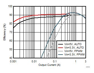 Figure 8-2 Buck
Efficiency in PFM/PWM and Forced PWM Mode
 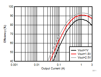 Figure 8-4 Buck
Efficiency in Forced PWM Mode
 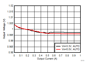 Figure 8-6 Buck
Output Voltage vs Load Current in PFM/PWM Mode
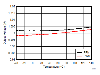
| Load
= 1 A (PWM) and 0.1 A (PFM) |
|
Figure 8-8 Buck
Output Voltage vs Temperature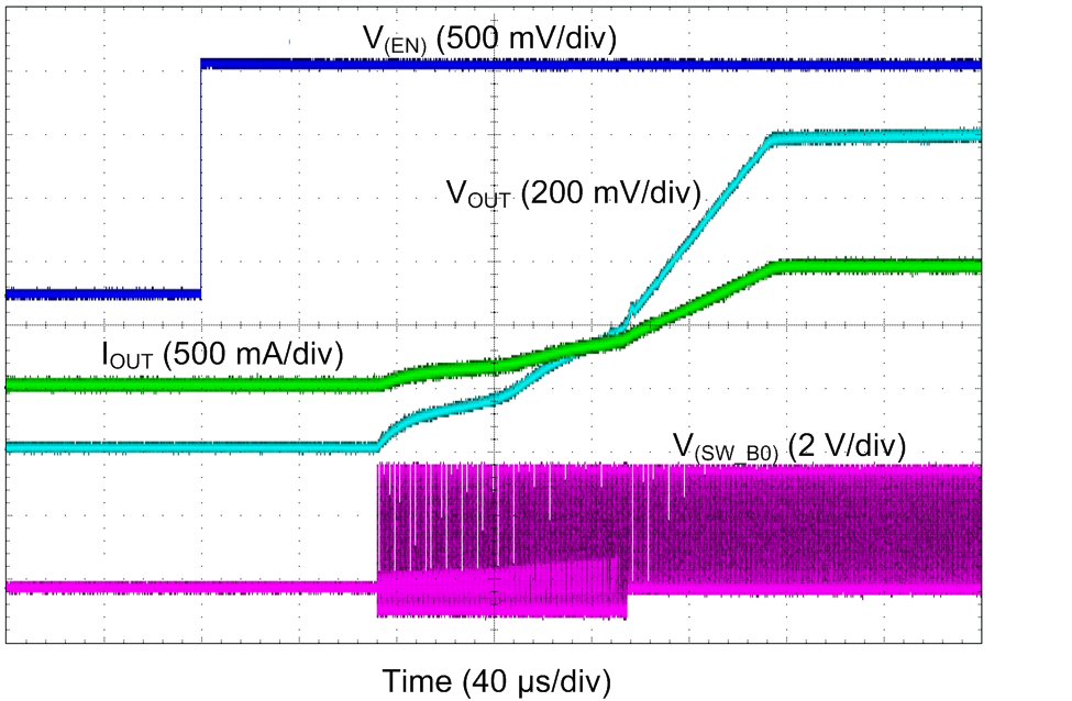
| Slew-rate = 10 mV/µs |
RLOAD = 1
Ω |
VOUT = 1
V |
Figure 8-10 Buck
Start-Up with EN1, Forced PWM Mode 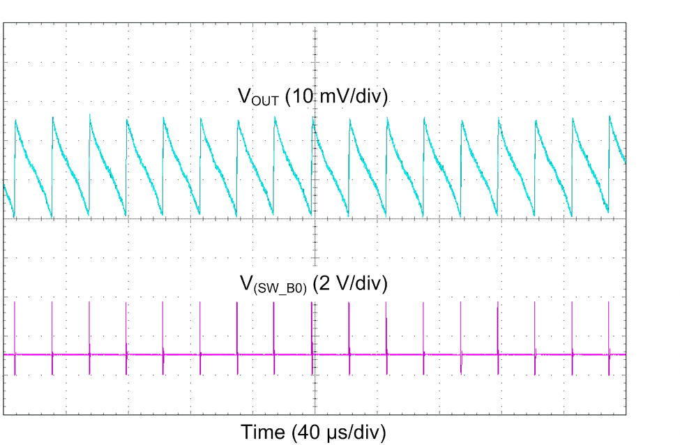 Figure 8-12 Buck
Output Voltage Ripple, PFM Mode
 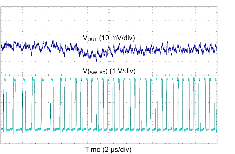 Figure 8-14 Buck
Transient From PFM-to-PWM Mode
| IOUT = 0.1 A → 2 A
→ 0.1 A |
TR =
TF = 400 ns |
|
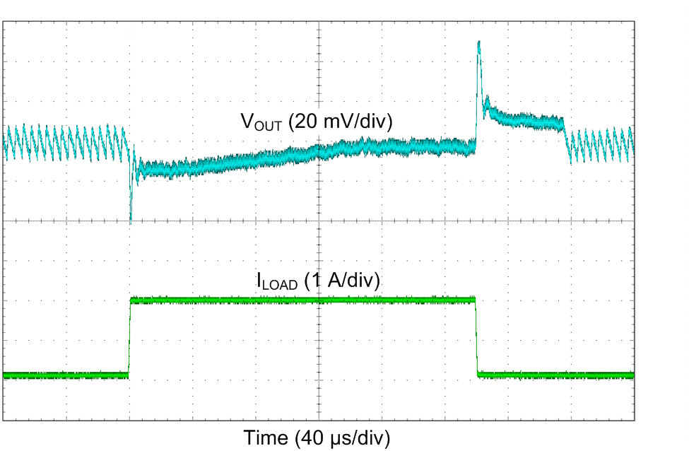
Figure 8-16 Buck
Transient Load Step Response, AUTO Mode 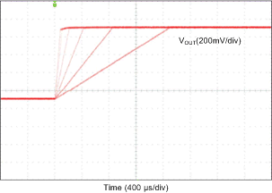 Figure 8-18 Buck
VOUT Transition from 0.6 V to 1.4 V With Different Slew Rate
Settings
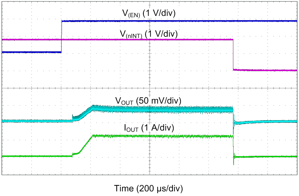 Figure 8-20 Buck
Start-Up With Short on Output
 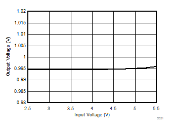 Figure 8-22 LDO
Output Voltage vs Input Voltage
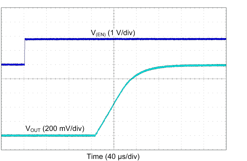 Figure 8-24 LDO
Start-Up
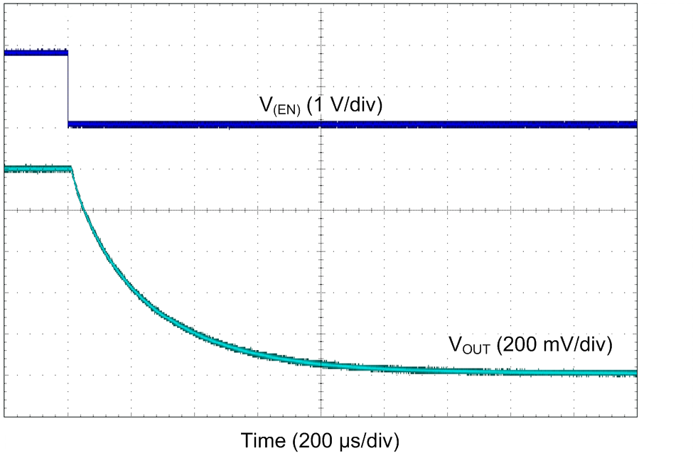 Figure 8-26 LDO
Shutdown
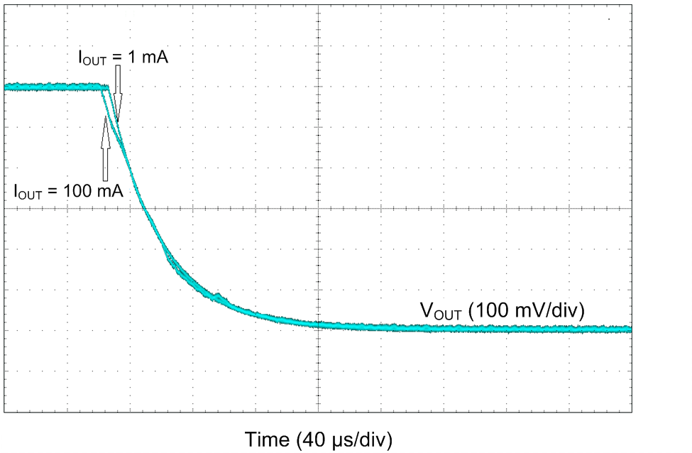 Figure 8-28 LDO
VOUT Transition from 1.8 V to 1.2 V
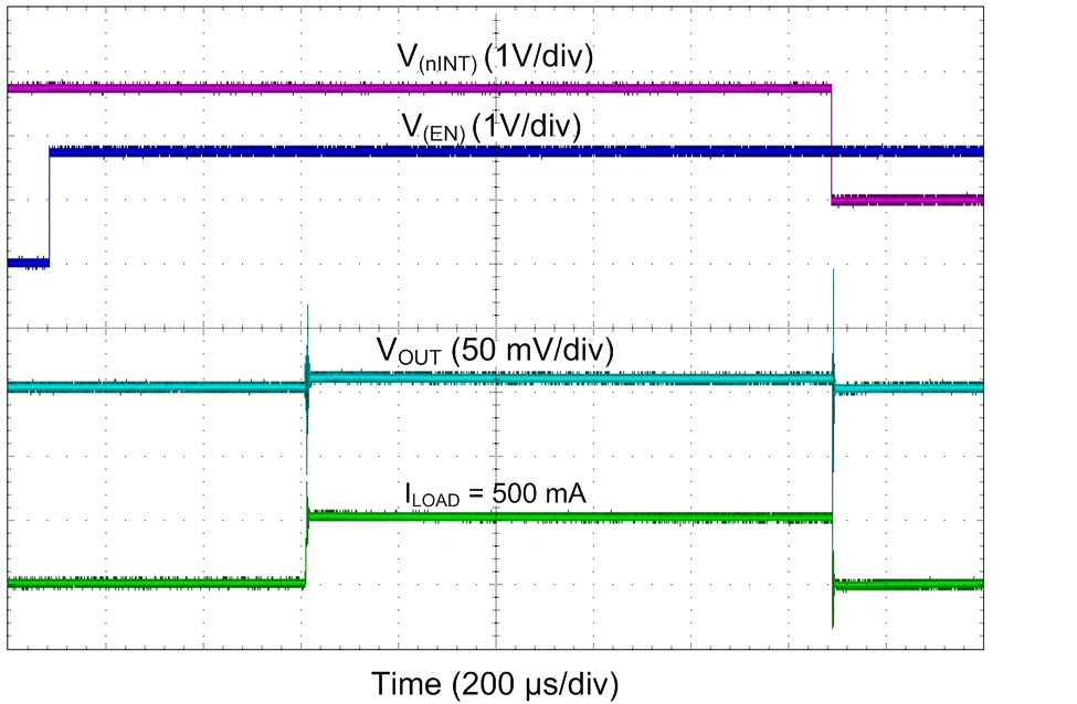 Figure 8-30 LDO
Start-Up With Short on Output
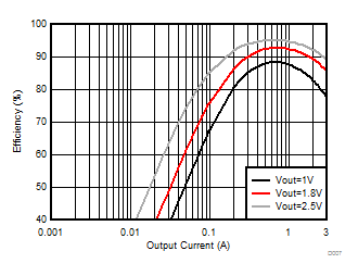 Figure 8-3 Buck
Efficiency in Forced PWM Mode
 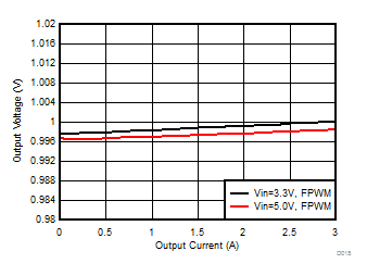 Figure 8-5 Buck
Output Voltage vs Load Current in Forced PWM Mode
 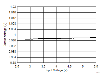 Figure 8-7 Buck
Output Voltage vs Input Voltage in PWM Mode
| Slew-rate = 10 mV/µs |
ILOAD = 0
A |
VOUT = 1
V |
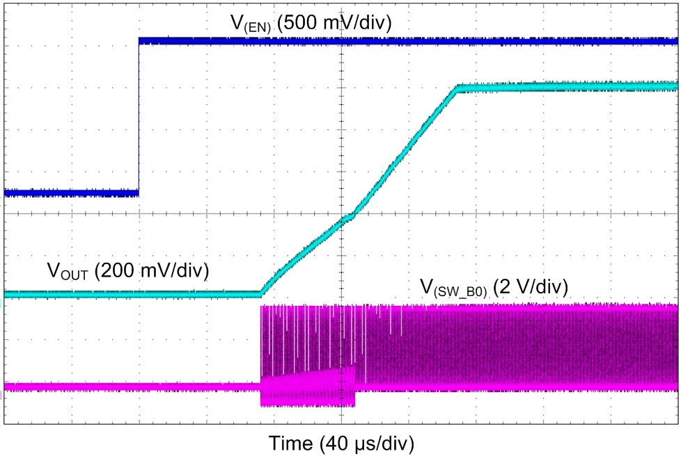
Figure 8-9 Buck
Start-Up With EN1, Forced PWM Mode 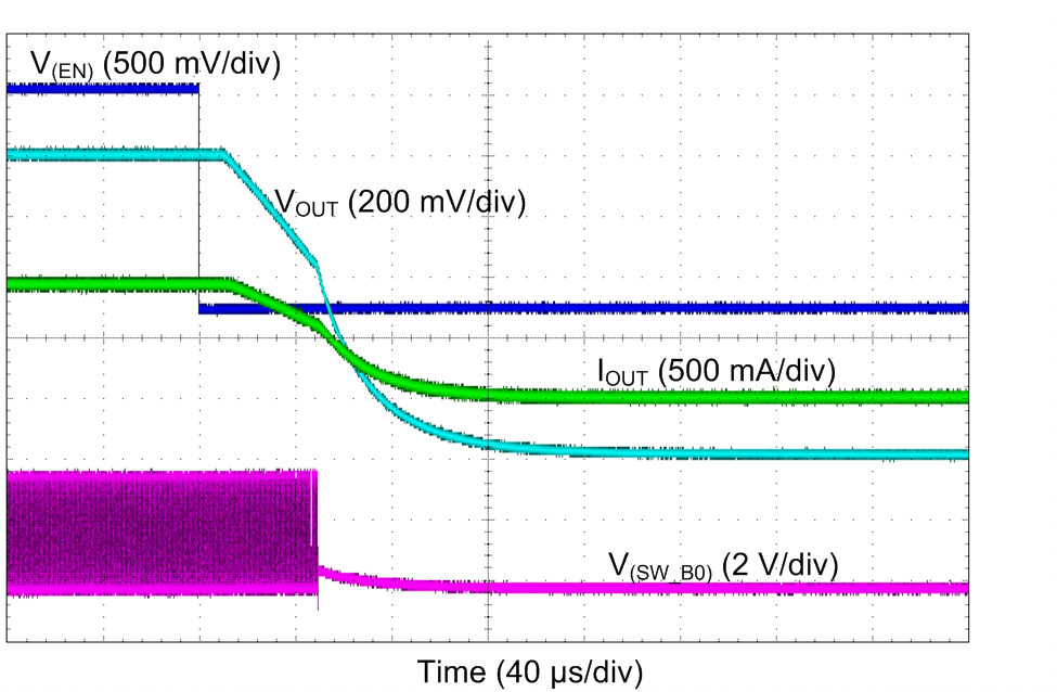
| Slew-rate = 10 mV/µs |
RLOAD = 1
Ω |
VOUT = 1
V |
Figure 8-11 Buck
Shutdown With EN1, Forced PWM Mode 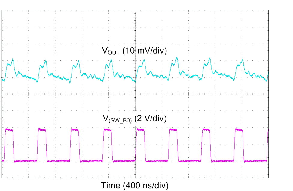 Figure 8-13 Buck
Output Voltage Ripple, Forced PWM Mode
 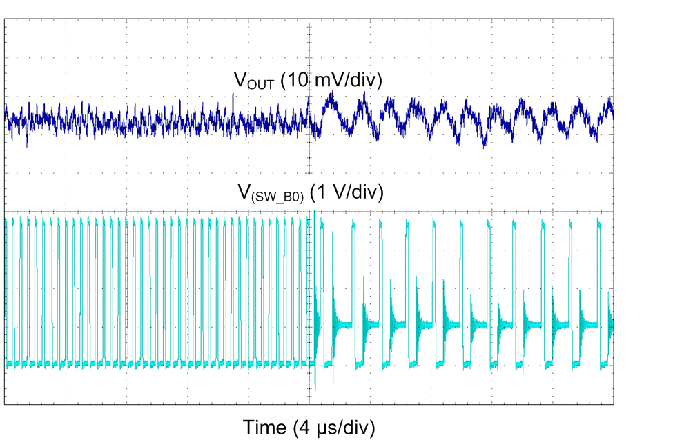 Figure 8-15 Buck
Transient From PWM-to-PFM Mode
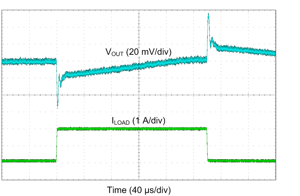
| IOUT = 0.1 A → 2 A
→ 0.1 A |
TR =
TF = 400 ns |
|
Figure 8-17 Buck
Transient Load Step Response, Forced PWM Mode 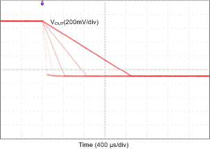 Figure 8-19 Buck
VOUT Transition from 1.4 V to 0.6 V With Different Slew Rate
Settings
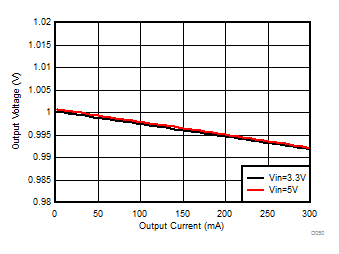 Figure 8-21 LDO
Output Voltage vs Load Current
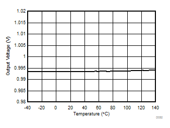 Figure 8-23 LDO
Output Voltage vs Temperature
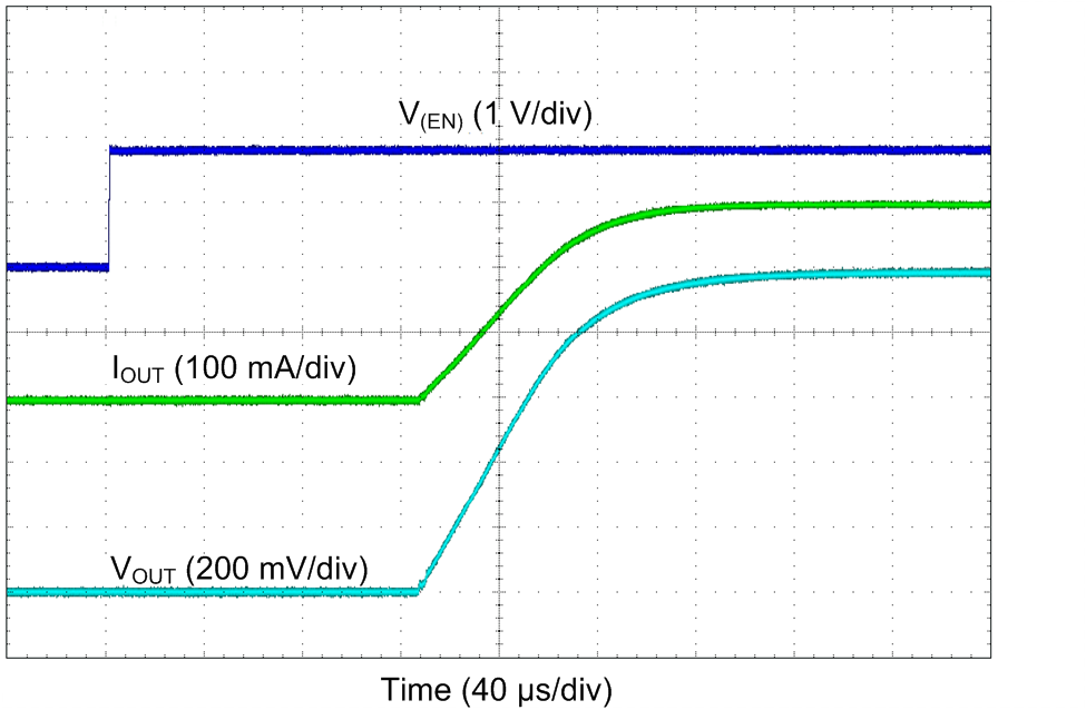 Figure 8-25 LDO
Start-Up
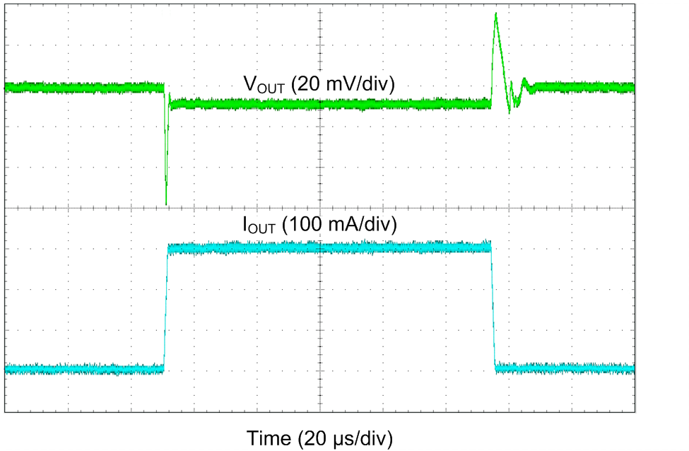
| IOUT = 0 A → 0.3 A → 0 A |
TR =
TF = 1 µs |
Figure 8-27 LDO
Transient Load Step Response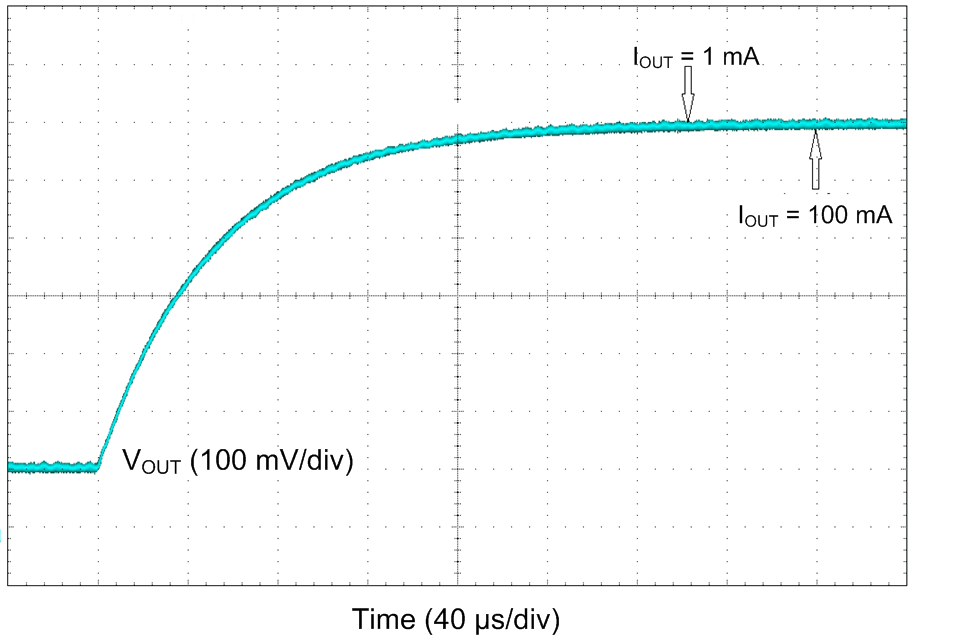 Figure 8-29 LDO
VOUT Transition from 1.2 V to 1.8 V


 Figure 8-14 Buck
Transient From PFM-to-PWM Mode
 Figure 8-18 Buck
VOUT Transition from 0.6 V to 1.4 V With Different Slew Rate
Settings
 Figure 8-20 Buck
Start-Up With Short on Output


 Figure 8-28 LDO
VOUT Transition from 1.8 V to 1.2 V


 Figure 8-15 Buck
Transient From PWM-to-PFM Mode
 Figure 8-19 Buck
VOUT Transition from 1.4 V to 0.6 V With Different Slew Rate
Settings


 Figure 8-29 LDO
VOUT Transition from 1.2 V to 1.8 V