SNVSC24 April   2021 LP8758-EA

PRODUCTION DATA  

  1. Features
  2. Applications
  3. Description
  4. Revision History
  5. Pin Configuration and Functions
  6. Specifications
    1. 6.1 Absolute Maximum Ratings
    2. 6.2 ESD Ratings
    3. 6.3 Recommended Operating Conditions
    4. 6.4 Thermal Information
    5. 6.5 Electrical Characteristics
    6. 6.6 I2C Serial Bus Timing Requirements
    7. 6.7 Switching Characteristics
    8. 6.8 Typical Characteristics
  7. Detailed Description
    1. 7.1 Overview
      1. 7.1.1 Buck Information
        1. 7.1.1.1 Operating Modes
        2. 7.1.1.2 Programmability
        3. 7.1.1.3 Features
    2. 7.2 Functional Block Diagram
    3. 7.3 Feature Description
      1. 7.3.1 Overview
        1. 7.3.1.1 Transition Between PWM and PFM Modes
        2. 7.3.1.2 Buck Converter Load Current Measurement
        3. 7.3.1.3 Spread-Spectrum Mode
      2. 7.3.2 Power-Up
      3. 7.3.3 Regulator Control
        1. 7.3.3.1 Enabling and Disabling
        2. 7.3.3.2 Changing Output Voltage
      4. 7.3.4 Device Reset Scenarios
      5. 7.3.5 Diagnosis and Protection Features
        1. 7.3.5.1 Warnings for Diagnosis (Interrupt)
          1. 7.3.5.1.1 Output Current Limit
          2. 7.3.5.1.2 Thermal Warning
        2. 7.3.5.2 Protection (Regulator Disable)
          1. 7.3.5.2.1 Short-Circuit and Overload Protection
          2. 7.3.5.2.2 Thermal Shutdown
        3. 7.3.5.3 Fault (Power Down)
          1. 7.3.5.3.1 Undervoltage Lockout
      6. 7.3.6 Digital Signal Filtering
    4. 7.4 Device Functional Modes
      1. 7.4.1 Modes of Operation
    5. 7.5 Programming
      1. 7.5.1 I2C-Compatible Interface
        1. 7.5.1.1 Data Validity
        2. 7.5.1.2 Start and Stop Conditions
        3. 7.5.1.3 Transferring Data
        4. 7.5.1.4 I2C-Compatible Chip Address
        5. 7.5.1.5 Auto Increment Feature
    6. 7.6 Register Maps
      1. 7.6.1 Register Descriptions
        1. 7.6.1.1  OTP_REV
        2. 7.6.1.2  BUCK0_CTRL1
        3. 7.6.1.3  BUCK0_CTRL2
        4. 7.6.1.4  BUCK1_CTRL1
        5. 7.6.1.5  BUCK1_CTRL2
        6. 7.6.1.6  BUCK2_CTRL1
        7. 7.6.1.7  BUCK2_CTRL2
        8. 7.6.1.8  BUCK3_CTRL1
        9. 7.6.1.9  BUCK3_CTRL2
        10. 7.6.1.10 BUCK0_VOUT
        11. 7.6.1.11 BUCK0_FLOOR_VOUT
        12. 7.6.1.12 BUCK1_VOUT
        13. 7.6.1.13 BUCK1_FLOOR_VOUT
        14. 7.6.1.14 BUCK2_VOUT
        15. 7.6.1.15 BUCK2_FLOOR_VOUT
        16. 7.6.1.16 BUCK3_VOUT
        17. 7.6.1.17 BUCK3_FLOOR_VOUT
        18. 7.6.1.18 BUCK0_DELAY
        19. 7.6.1.19 BUCK1_DELAY
        20. 7.6.1.20 BUCK2_DELAY
        21. 7.6.1.21 BUCK3_DELAY
        22. 7.6.1.22 RESET
        23. 7.6.1.23 CONFIG
        24. 7.6.1.24 INT_TOP
        25. 7.6.1.25 INT_BUCK_0_1
        26. 7.6.1.26 INT_BUCK_2_3
        27. 7.6.1.27 TOP_STAT
        28. 7.6.1.28 BUCK_0_1_STAT
        29. 7.6.1.29 BUCK_2_3_STAT
        30. 7.6.1.30 TOP_MASK
        31. 7.6.1.31 BUCK_0_1_MASK
        32. 7.6.1.32 BUCK_2_3_MASK
        33. 7.6.1.33 SEL_I_LOAD
        34. 7.6.1.34 I_LOAD_2
        35. 7.6.1.35 I_LOAD_1
  8. Application and Implementation
    1. 8.1 Application Information
    2. 8.2 Typical Application
      1. 8.2.1 Design Requirements
      2. 8.2.2 Detailed Design Procedure
        1. 8.2.2.1 Application Components
          1. 8.2.2.1.1 Inductor Selection
          2. 8.2.2.1.2 Input Capacitor Selection
          3. 8.2.2.1.3 Output Capacitor Selection
      3. 8.2.3 Application Curves
  9. Power Supply Recommendations
  10. 10Layout
    1. 10.1 Layout Guidelines
    2. 10.2 Layout Example
  11. 11Device and Documentation Support
    1. 11.1 Device Support
    2. 11.2 Documentation Support
      1. 11.2.1 Related Documentation
    3. 11.3 Receiving Notification of Documentation Updates
    4. 11.4 Support Resources
    5. 11.5 Trademarks
    6. 11.6 Electrostatic Discharge Caution
    7. 11.7 Glossary
  12. 12Mechanical, Packaging, and Orderable Information

Package Options

Mechanical Data (Package|Pins)
Thermal pad, mechanical data (Package|Pins)
Orderable Information

Description

The LP8758-EA device is designed to meet power management requirements for low-power processors in mobile phones, network cards, and similar applications. The device contains four step-down DC-DC converter cores, providing four output voltage rails. The device is controlled by an I2C-compatible serial interface.

The automatic PWM-PFM (AUTO mode) operation maximizes efficiency over a wide output-current range.

The LP8758-EA supports programmable start-up and shutdown sequencing synchronized to hardware Enable input signal.

The protection features include short-circuit protection, current limits, input supply UVLO, and temperature warning and shutdown functions. Several error flags are provided for status information of the device. In addition, the LP8758-EA device supports load current measurement without the addition of external current sense resistors. During start-up and voltage change, the device controls the output slew rate to minimize output voltage overshoot and the inrush current.

Device Information(1)
PART NUMBER DEFAULT OUTPUT VOLTAGE
LP8758-EA VOUT0 800 mV
VOUT1 800 mV
VOUT2 800 mV
VOUT3 800 mV
For all available packages, see the orderable addendum at the end of the data sheet.
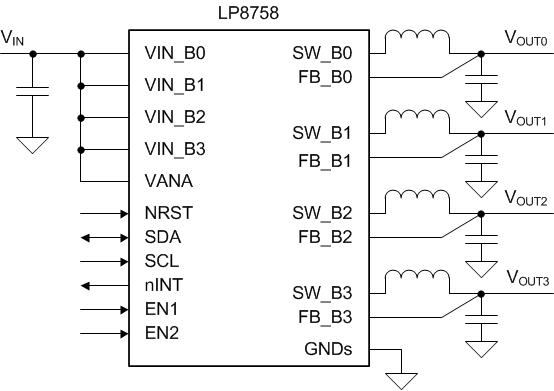
GUID-07B69527-6EB2-46DD-95E0-BE963B4A911D-low.gifSimplified Schematic
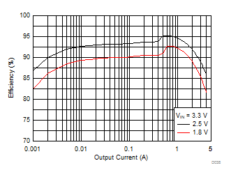
GUID-12C64B02-68E5-4B02-B3ED-FB270001A439-low.gif
VOUT settings = 1.8 V and 2.5 V
Efficiency vs Output Current