SNVSAZ9 March   2022 LP8764-Q1

PRODUCTION DATA  

  1. Features
  2. Applications
  3. Description
  4. Revision History
  5. Pin Configuration and Functions
    1. 5.1 Digital Signal Descriptions
  6. Specifications
    1. 6.1  Absolute Maximum Ratings
    2. 6.2  ESD Ratings
    3. 6.3  Recommended Operating Conditions
    4. 6.4  Thermal Information
    5. 6.5  Internal Low Drop-Out Regulators (LDOVINT)
    6. 6.6  BUCK1, BUCK2, BUCK3, and BUCK4 Regulators
    7. 6.7  Reference Generator (REFOUT)
    8. 6.8  Monitoring Functions
    9. 6.9  Clocks, Oscillators, and DPLL
    10. 6.10 Thermal Monitoring and Shutdown
    11. 6.11 System Control Thresholds
    12. 6.12 Current Consumption
    13. 6.13 Digital Input Signal Parameters
    14. 6.14 Digital Output Signal Parameters
    15. 6.15 I/O Pullup and Pulldown Resistance
    16. 6.16 I2C Interface
    17. 6.17 Serial Peripheral Interface (SPI)
      1.      25
  7. Typical Characteristics
  8. Detailed Description
    1. 8.1  Overview
    2. 8.2  Functional Block Diagram
    3. 8.3  Input Voltage Monitor
    4. 8.4  Device State Machine
      1. 8.4.1 Fixed Device Power FSM
        1. 8.4.1.1 Register Resets and EEPROM read at INIT state
      2. 8.4.2 Pre-Configurable Mission States
        1. 8.4.2.1 PFSM Commands
          1. 8.4.2.1.1  REG_WRITE_IMM Command
          2. 8.4.2.1.2  REG_WRITE_MASK_IMM Command
          3. 8.4.2.1.3  REG_WRITE_MASK_PAGE0_IMM Command
          4. 8.4.2.1.4  REG_WRITE_BIT_PAGE0_IMM Command
          5. 8.4.2.1.5  REG_WRITE_WIN_PAGE0_IMM Command
          6. 8.4.2.1.6  REG_WRITE_VOUT_IMM Command
          7. 8.4.2.1.7  REG_WRITE_VCTRL_IMM Command
          8. 8.4.2.1.8  REG_WRITE_MASK_SREG Command
          9. 8.4.2.1.9  SREG_READ_REG Command
          10. 8.4.2.1.10 SREG_WRITE_IMM Command
          11. 8.4.2.1.11 WAIT Command
          12. 8.4.2.1.12 DELAY_IMM Command
          13. 8.4.2.1.13 DELAY_SREG Command
          14. 8.4.2.1.14 TRIG_SET Command
          15. 8.4.2.1.15 TRIG_MASK Command
          16. 8.4.2.1.16 END Command
        2. 8.4.2.2 Configuration Memory Organization and Sequence Execution
        3. 8.4.2.3 Mission State Configuration
        4. 8.4.2.4 Pre-Configured Hardware Transitions
          1. 8.4.2.4.1 ON Requests
          2. 8.4.2.4.2 OFF Requests
            1. 8.4.2.4.2.1 NSLEEP1 and NSLEEP2 Functions
            2. 8.4.2.4.2.2 WKUP1 and WKUP2 Functions
      3. 8.4.3 Error Handling Operations
        1. 8.4.3.1 Power Rail Output Error
        2. 8.4.3.2 Boot BIST Error
        3. 8.4.3.3 Runtime BIST Error
        4. 8.4.3.4 Catastrophic Error
        5. 8.4.3.5 Watchdog (WDOG) Error
        6. 8.4.3.6 Error Signal Monitor (ESM) Error
        7. 8.4.3.7 Warnings
      4. 8.4.4 Device Start-up Timing
      5. 8.4.5 Power Sequences
      6. 8.4.6 First Supply Detection
    5. 8.5  Power Resources
      1. 8.5.1 Buck Regulators
        1. 8.5.1.1 BUCK Regulator Overview
        2. 8.5.1.2 Multi-Phase Operation and Phase-Adding or Shedding
        3. 8.5.1.3 Transition Between PWM and PFM Modes
        4. 8.5.1.4 Spread-Spectrum Mode
        5. 8.5.1.5 Adaptive Voltage Scaling (AVS) and Dynamic Voltage Scaling (DVS) Support
        6. 8.5.1.6 BUCK Output Voltage Setting
      2. 8.5.2 Sync Clock Functionality
      3. 8.5.3 Internal Low Dropout Regulator (LDOVINT)
    6. 8.6  Residual Voltage Checking
    7. 8.7  Output Voltage Monitor and PGOOD Generation
    8. 8.8  General-Purpose I/Os (GPIO Pins)
    9. 8.9  Thermal Monitoring
      1. 8.9.1 Thermal Warning Function
      2. 8.9.2 Thermal Shutdown
    10. 8.10 Interrupts
    11. 8.11 Control Interfaces
      1. 8.11.1 CRC Calculation for I2C and SPI Interface Protocols
      2. 8.11.2 I2C-Compatible Interface
        1. 8.11.2.1 Data Validity
        2. 8.11.2.2 Start and Stop Conditions
        3. 8.11.2.3 Transferring Data
        4. 8.11.2.4 Auto-Increment Feature
      3. 8.11.3 Serial Peripheral Interface (SPI)
    12. 8.12 Multi-PMIC Synchronization
      1. 8.12.1 SPMI Interface System Setup
      2. 8.12.2 Transmission Protocol and CRC
        1. 8.12.2.1 Operation with Transmission Errors
        2. 8.12.2.2 Transmitted Information
      3. 8.12.3 SPMI Target Device Communication to SPMI Controller Device
        1. 8.12.3.1 Incomplete Communication from SPMI Target Device to SPMI Controller Device
      4. 8.12.4 SPMI-BIST Overview
        1. 8.12.4.1 SPMI Bus during Boot BIST and RUNTIME BIST
        2. 8.12.4.2 Periodic Checking of the SPMI
        3. 8.12.4.3 SPMI Message Priorities
    13. 8.13 NVM Configurable Registers
      1. 8.13.1 Register Page Partitioning
      2. 8.13.2 CRC Protection for Configuration, Control, and Test Registers
      3. 8.13.3 CRC Protection for User Registers
      4. 8.13.4 Register Write Protection
        1. 8.13.4.1 ESM and WDOG Configuration Registers
        2. 8.13.4.2 User Registers
    14. 8.14 Watchdog (WD)
      1. 8.14.1 Watchdog Fail Counter and Status
      2. 8.14.2 Watchdog Start-Up and Configuration
      3. 8.14.3 MCU to Watchdog Synchronization
      4. 8.14.4 Watchdog Disable Function
      5. 8.14.5 Watchdog Sequence
      6. 8.14.6 Watchdog Trigger Mode
      7. 8.14.7 WatchDog Flow Chart and Timing Diagrams in Trigger Mode
      8.      121
      9. 8.14.8 Watchdog Question-Answer Mode
        1. 8.14.8.1 Watchdog Q&A Related Definitions
        2. 8.14.8.2 Question Generation
        3. 8.14.8.3 Answer Comparison
          1. 8.14.8.3.1 Sequence of the 2-bit Watchdog Answer Counter
          2. 8.14.8.3.2 Watchdog Sequence Events and Status Updates
          3. 8.14.8.3.3 Watchdog Q&A Sequence Scenarios
    15. 8.15 Error Signal Monitor (ESM)
      1. 8.15.1 ESM Error-Handling Procedure
      2. 8.15.2 Level Mode
      3.      132
      4. 8.15.3 PWM Mode
        1. 8.15.3.1 Good-Events and Bad-Events
        2. 8.15.3.2 ESM Error-Counter
          1. 8.15.3.2.1 ESM Start-Up in PWM Mode
        3. 8.15.3.3 ESM Flow Chart and Timing Diagrams in PWM Mode
        4.       138
    16. 8.16 Register Map
      1. 8.16.1 LP8764x_map Registers
  9. Application and Implementation
    1. 9.1 Application Information
    2. 9.2 Typical Applications
      1. 9.2.1 Design Requirements
        1. 9.2.1.1 Buck Inductor Selection
        2. 9.2.1.2 Buck Input Capacitor Selection
        3. 9.2.1.3 Buck Output Capacitor Selection
        4. 9.2.1.4 LDO Output Capacitor Selection
        5. 9.2.1.5 VCCA Supply Filtering Components
      2. 9.2.2 Detailed Design Procedure
      3. 9.2.3 Voltage Scaling Precautions
      4. 9.2.4 Application Curves
  10. 10Power Supply Recommendations
  11. 11Layout
    1. 11.1 Layout Guidelines
    2. 11.2 Layout Example
  12. 12Device and Documentation Support
    1. 12.1 Receiving Notification of Documentation Updates
    2. 12.2 Support Resources
    3. 12.3 Trademarks
    4. 12.4 Electrostatic Discharge Caution
    5. 12.5 Glossary
  13. 13Mechanical, Packaging, and Orderable Information

Package Options

Mechanical Data (Package|Pins)
Thermal pad, mechanical data (Package|Pins)
Orderable Information

SPMI-BIST Overview

The SPMI-BIST is performed during BIST state and regularly during runtime operation. Figure 8-40 below illustrates how the SPMI-BIST operates during device power-up.
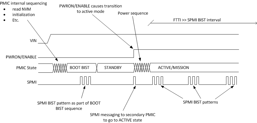
GUID-D69C5CA7-D554-43B8-A997-6D859216DF7B-low.gifFigure 8-40 SPMI-BIST Operation

After the input power is detected and verified to be at the correct level, the LP8764-Q1 initializes itself by reading the NVM and performs all actions that are needed to prepare for operation . After this initialization, the LP8764-Q1 enters the BOOT BIST state, in which the internal logic performs a series of tests to verify that the LP8764-Q1 device is OK. As part of this test, the SPMI- BIST is performed. After it is completed successfully, the LP8764-Q1 device goes to the standby state and waits for further signals from the system to initiate the power-up sequence of the processor.

A valid on request initiates the processor power-up sequence. The controller device communicates this event through the SPMI bus to all of the target devices. After that, the power-up sequence is executed and LP8764-Q1 enters the configured mission state.