SNVSBU3 March 2021 LP87702
PRODUCTION DATA
- 1 Features
- 2 Applications
- 3 Description
- 4 Revision History
- 5 Pin Configuration and Functions
- 6 Specifications
-
7 Detailed Description
- 7.1 Overview
- 7.2 Functional Block Diagram
- 7.3
Feature Descriptions
- 7.3.1 Step-Down DC/DC Converters
- 7.3.2 Boost Converter
- 7.3.3 Spread-Spectrum Mode
- 7.3.4 Sync Clock Functionality
- 7.3.5 Power-Up
- 7.3.6 Buck and Boost Control
- 7.3.7 Enable and Disable Sequences
- 7.3.8 Window Watchdog
- 7.3.9 Device Reset Scenarios
- 7.3.10 Diagnostics and Protection Features
- 7.3.11 OTP Error Correction
- 7.3.12 Operation of GPO Signals
- 7.3.13 Digital Signal Filtering
- 7.4 Device Functional Modes
- 7.5 Programming
- 7.6 Register Maps
- 8 Application and Implementation
- 9 Power Supply Recommendations
- 10Layout
- 11Device and Documentation Support
- 12Mechanical, Packaging, and Orderable Information
Package Options
Mechanical Data (Package|Pins)
- RHB|32
Thermal pad, mechanical data (Package|Pins)
- RHB|32
Orderable Information
7.3.7 Enable and Disable Sequences
The LP87702 device supports programmable start-up and shutdown sequencing. An enable control signal is used to initiate the start-up sequence and to turn off the device according to the programmed shutdown sequence. Up to three enable inputs are available: EN1 is a dedicated enable input; EN2 and EN3 are multiplexed with I2C interface. The buck converter is selected for sequence control with:
- BUCKx_CTRL_1(BUCKx_EN) = 1
- BUCKx_CTRL_1(BUCKx_EN_PIN_CTRL) = 0x1 or 0x2 or 0x3, for EN1 or EN2 or EN3 control, respectively
- BUCKx_VOUT.(BUCKx_VSET[7:0]) = Required voltage when EN pin is high
- The delay from rising edge of EN pin to the converter enable is set by BUCKx_DELAY(BUCKx_STARTUP_DELAY[3:0]) bits and
- The delay from falling edge of EN pin to the converter disable is set by BUCKx_DELAY(BUCKx_SHUTDOWN_DELAY[3:0])
In the same way the boost converter is selected for delayed control with:
- BOOST_CTRL(BOOST_EN) = 1
- BOOST_CTRL(BOOST_EN_PIN_CTRL) = 0x1 or 0x2 or 0x3, for EN1. EN2, or EN3 control (respectively)
- BOOST_CTRL(BOOST_VSET[2:0]) = Required voltage when EN pin is high
- The delay from rising edge of EN pin to the converter enable is set by BOOST_DELAY(BOOST_STARTUP_DELAY[3:0]) bits and
- The delay from falling edge of EN pin to the converter disable is set by BOOST_DELAY(BOOST_SHUTDOWN_DELAY[3:0])
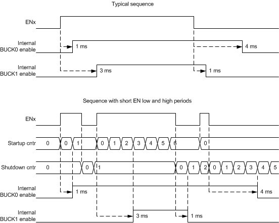
An example of start-up and shutdown sequences for buck converters are shown in Figure 7-7. The start-up and shutdown delays for Buck0 converter are 1 ms and 4 ms and for Buck1 converter 3 ms and 1 ms. The delay settings are used only for enable or disable control with the EN signal.
 Figure 7-7 Start-up and Shutdown Sequencing Example