SNVSBD1A August 2020 – February 2021 LP8866S-Q1
PRODUCTION DATA
- 1 Features
- 2 Applications
- 3 Description
- 4 Revision History
- 5 Pin Configuration and Functions
- 6 Specifications
-
7 Detailed Description
- 7.1 Overview
- 7.2 Functional Block Diagram
- 7.3
Feature Description
- 7.3.1 Control Interface
- 7.3.2 Function Setting
- 7.3.3 Device Supply (VDD)
- 7.3.4 Enable (EN)
- 7.3.5 Charge Pump
- 7.3.6 Boost Controller
- 7.3.7 LED Current Sinks
- 7.3.8 Brightness Control
- 7.3.9
Protection and Fault Detections
- 7.3.9.1 Supply Faults
- 7.3.9.2
Boost Faults
- 7.3.9.2.1 Boost Overvoltage Faults (BSTOVPL, BSTOVPH)
- 7.3.9.2.2 Boost Overcurrent Faults (BSTOCP)
- 7.3.9.2.3 LEDSET Resistor Missing Faults (LEDSET)
- 7.3.9.2.4 MODE Resistor Missing Faults (MODESEL)
- 7.3.9.2.5 FSET Resistor Missing Faults (FSET)
- 7.3.9.2.6 ISET Resistor Out of Range Faults (ISET)
- 7.3.9.2.7 Thermal Shutdown Faults (TSD)
- 7.3.9.3 LED Faults
- 7.3.9.4 Overview of the Fault and Protection Schemes
- 7.4 Device Functional Modes
- 7.5 Programming
- 7.6 Register Maps
-
8 Application and Implementation
- 8.1 Application Information
- 8.2
Typical Applications
- 8.2.1
Full Feature Application for Display Backlight
- 8.2.1.1 Design Requirements
- 8.2.1.2
Detailed Design Procedure
- 8.2.1.2.1 Inductor Selection
- 8.2.1.2.2 Output Capacitor Selection
- 8.2.1.2.3 Input Capacitor Selection
- 8.2.1.2.4 Charge Pump Output Capacitor
- 8.2.1.2.5 Charge Pump Flying Capacitor
- 8.2.1.2.6 Output Diode
- 8.2.1.2.7 Switching FET
- 8.2.1.2.8 Boost Sense Resistor
- 8.2.1.2.9 Power-Line FET
- 8.2.1.2.10 Input Current Sense Resistor
- 8.2.1.2.11 Feedback Resistor Divider
- 8.2.1.2.12 Critical Components for Design
- 8.2.1.3 Application Curves
- 8.2.2 Application with Basic/Minimal Operation
- 8.2.3
SEPIC Mode Application
- 8.2.3.1 Design Requirements
- 8.2.3.2
Detailed Design Procedure
- 8.2.3.2.1 Inductor Selection
- 8.2.3.2.2 Coupling Capacitor Selection
- 8.2.3.2.3 Output Capacitor Selection
- 8.2.3.2.4 Input Capacitor Selection
- 8.2.3.2.5 Charge Pump Output Capacitor
- 8.2.3.2.6 Charge Pump Flying Capacitor
- 8.2.3.2.7 Switching FET
- 8.2.3.2.8 Output Diode
- 8.2.3.2.9 Switching Sense Resistor
- 8.2.3.2.10 Power-Line FET
- 8.2.3.2.11 Input Current Sense Resistor
- 8.2.3.2.12 Feedback Resistor Divider
- 8.2.3.2.13 Critical Components for Design
- 8.2.3.3 Application Curves
- 8.2.1
Full Feature Application for Display Backlight
- 9 Power Supply Recommendations
- 10Layout
- 11Device and Documentation Support
- 12Mechanical, Packaging, and Orderable Information
Package Options
Mechanical Data (Package|Pins)
Thermal pad, mechanical data (Package|Pins)
Orderable Information
7.3.6.3.1 FB Divider Using Two-Resistor Method
A typical FB-pin circuit uses a two-resistor divider circuit between the boost output voltage and ground.
 Figure 7-5 Two-Resistor FB Divider Circuit
Maximum boost voltage can be calculated with Equation 2. The maximum boost voltage can be reached during OPEN string detection or if all LED strings are left disconnected.

where
- VREF= 1.21 V
- ISEL_MAX = 38.7 µA
- R1 / R2 normal recommended range is 7~15
The minimum boost voltage must be less than the minimum LED string voltage. Minimum boost voltage is calculated with Equation 3:

where
- VREF = 1.21 V
When the boost OVP_LOW level is reached, the boost controller stops switching the boost FET and the BSTOVPL_STATUS bit is set. The LED drivers are still active during this condition, and the boost resumes normal switching operation once the boost output level falls. The boost OVP low voltage threshold changes dynamically with current boost voltage. It is calculated in Equation 4:

where
- VFB_OVPL = 1.423 V
- VREF = 1.21 V
When the boost OVP_HIGH level is reached the boost controller enters fault recovery mode, and the BSTOVPH_STATUS bit is set. The boost OVP high-voltage threshold also changes dynamically with current boost voltage and is calculated in Equation 5:
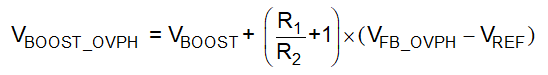
where
- VFB_OVPH = 1.76 V
- VREF = 1.21 V
When the boost UVP level is reached the boost controller starts a 110-ms OCP counter. The LP8866S-Q1 device enters the fault recovery mode and sets the BSTOCP_STATUS bit if the boost voltage does not rise above the UVP threshold before the timer expires. The boost UVP voltage threshold also changes dynamically with current boost voltage and is calculated in Equation 6:

where
- VUVP = 0.886 V
- VREF = 1.21 V