SNVSB83B June 2019 – January 2020 LP8867-Q1 , LP8869-Q1
PRODUCTION DATA.
- 1 Features
- 2 Applications
- 3 Description
- 4 Revision History
- 5 Device Comparison Table
- 6 Pin Configuration and Functions
-
7 Specifications
- 7.1 Absolute Maximum Ratings
- 7.2 ESD Ratings
- 7.3 Recommended Operating Conditions
- 7.4 Thermal Information
- 7.5 Electrical Characteristics
- 7.6 Internal LDO Electrical Characteristics
- 7.7 Protection Electrical Characteristics
- 7.8 Current Sinks Electrical Characteristics
- 7.9 PWM Brightness Control Electrical Characteristics
- 7.10 Boost and SEPIC Converter Characteristics
- 7.11 Logic Interface Characteristics
- 7.12 Typical Characteristics
-
8 Detailed Description
- 8.1 Overview
- 8.2 Functional Block Diagram
- 8.3
Feature Description
- 8.3.1 Integrated DC-DC Converter
- 8.3.2 Internal LDO
- 8.3.3 LED Current Sinks
- 8.3.4 Power-Line FET Control
- 8.3.5 LED Current Dimming With External Temperature Sensor
- 8.3.6 Fault Detections and Protection
- 8.4 Device Functional Modes
- 9 Application and Implementation
- 10Power Supply Recommendations
- 11Layout
- 12Device and Documentation Support
- 13Mechanical, Packaging, and Orderable Information
Package Options
Mechanical Data (Package|Pins)
- PWP|20
Thermal pad, mechanical data (Package|Pins)
- PWP|20
Orderable Information
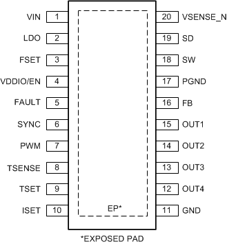
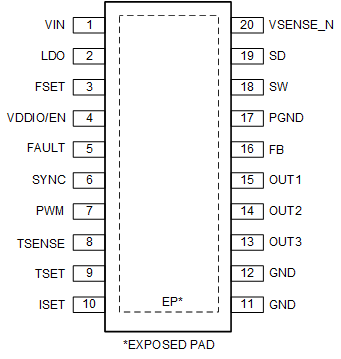
6 Pin Configuration and Functions
LP8867-Q1 PWP Package
20-Pin HTSSOP With Exposed Thermal Pad
Top View

LP8869-Q1 PWP Package
20-Pin HTSSOP With Exposed Thermal Pad
Top View

Pin Functions
| PIN | TYPE(1) | DESCRIPTION | |
|---|---|---|---|
| NO. | NAME | ||
| 1 | VIN | A | Input power pin; input voltage OVP detection pin; input current sense positive input pin. |
| 2 | LDO | A | Output of internal LDO; connect a 1-μF decoupling capacitor between this pin and noise-free ground. Put the capacitor as close to the chip as possible. |
| 3 | FSET | A | DC-DC (boost or SEPIC) switching frequency setting resistor; for normal operation, resistor value from 24 kΩ to 219 kΩ must be connected between this pin and ground. |
| 4 | VDDIO/EN | I | Enable input for the device as well as supply input (VDDIO) for digital pins. |
| 5 | FAULT | OD | Fault signal output. If unused, the pin may be left floating. |
| 6 | SYNC | I | Input for synchronizing DC-DC converter. If synchronization is not used, connect this pin to ground to disable spread spectrum or to VDDIO/EN to enable spread spectrum. |
| 7 | PWM | I | PWM dimming input. |
| 8 | TSENSE | A | Input for NTC resistor divider. Refer to LED Current Dimming With External Temperature Sensor for proper connection. If unused, the pin must be left floating. |
| 9 | TSET | A | Input for NTC resistor divider. Refer to LED Current Dimming With External Temperature Sensor for proper connection. If unused, the pin must be connected to GND. |
| 10 | ISET | A | LED current setting resistor; for normal operation, resistor value from 20 kΩ to 129 kΩ must be connected between this pin and ground. |
| 11 | GND | G | Ground. |
| 12 | OUT4/GND | A | Current sink output for LP8867-Q1
This pin must be connected to ground if not used. GND pin for LP8869-Q1 |
| 13 | OUT3 | A | Current sink output.
This pin must be connected to ground if not used. |
| 14 | OUT2 | A | Current sink output.
This pin must be connected to ground if not used. |
| 15 | OUT1 | A | Current sink output.
This pin must be connected to ground if not used. |
| 16 | FB | A | DC-DC (boost or SEPIC) feedback input; for normal operation this pin must be connected to the middle of a resistor divider between VOUT and ground using feedback resistor values greater than 5kΩ. |
| 17 | PGND | G | DC-DC (boost or SEPIC) power ground. |
| 18 | SW | A | DC-DC (boost or SEPIC) switch pin. |
| 19 | SD | A | Power-line FET control. Open Drain (current sink type) Output. If unused, the pin may be left floating. |
| 20 | VSENSE_N | A | Input current sense negative input. Connect to VIN pin when input current sense resistor is not used. |
(1) A: Analog pin, G: Ground pin, P: Power pin, I: Input pin, I/O: Input/Output pin, O: Output pin, OD: Open Drain pin