SNOSB14D August 2009 – December 2014 LPV521
PRODUCTION DATA.
- 1 Features
- 2 Applications
- 3 Description
- 4 Revision History
- 5 Pin Configuration and Functions
-
6 Specifications
- 6.1 Absolute Maximum Ratings
- 6.2 ESD Ratings
- 6.3 Recommended Operating Conditions
- 6.4 Thermal Information
- 6.5 1.8-V DC Electrical Characteristics
- 6.6 1.8-V AC Electrical Characteristics
- 6.7 3.3-V DC Electrical Characteristics
- 6.8 3.3-V AC Electrical Characteristics
- 6.9 5-V DC Electrical Characteristics
- 6.10 5-V AC Electrical Characteristics
- 6.11 Typical Characteristics
- 7 Detailed Description
- 8 Applications and Implementation
- 9 Power Supply Recommendations
- 10Layout
- 11Device and Documentation Support
- 12Mechanical, Packaging, and Orderable Information
Package Options
Mechanical Data (Package|Pins)
- DCK|5
Thermal pad, mechanical data (Package|Pins)
Orderable Information
8 Applications and Implementation
NOTE
Information in the following applications sections is not part of the TI component specification, and TI does not warrant its accuracy or completeness. TI’s customers are responsible for determining suitability of components for their purposes. Customers should validate and test their design implementation to confirm system functionality.
8.1 Application Information
The LPV521is specified for operation from 1.6 V to 5.5 V (±0.8 V to ±2.25 V). Many of the specifications apply from –40°C to 125°C. The LMV521 features rail to rail input and rail-to-rail output swings while consuming only nanowatts of power. Parameters that can exhibit significant variance with regard to operating voltage or temperature are presented in the Typical Characteristics section.
8.1.1 Driving Capacitive Load
The LPV521 is internally compensated for stable unity gain operation, with a 6.2-kHz, typical gain bandwidth. However, the unity gain follower is the most sensitive configuration to capacitive load. The combination of a capacitive load placed at the output of an amplifier along with the amplifier’s output impedance creates a phase lag, which reduces the phase margin of the amplifier. If the phase margin is significantly reduced, the response will be under damped which causes peaking in the transfer and, when there is too much peaking, the op amp might start oscillating.
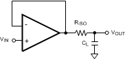 Figure 62. Resistive Isolation of Capacitive Load
In order to drive heavy capacitive loads, an isolation resistor, RISO, should be used, as shown in Figure 62. By using this isolation resistor, the capacitive load is isolated from the amplifier’s output. The larger the value of RISO, the more stable the amplifier will be. If the value of RISO is sufficiently large, the feedback loop will be stable, independent of the value of CL. However, larger values of RISO result in reduced output swing and reduced output current drive.
Recommended minimum values for RISO are given in the following table, for 5-V supply. Figure 63 shows the typical response obtained with the CL = 50 pF and RISO = 154 kΩ. The other values of RISO in the table were chosen to achieve similar dampening at their respective capacitive loads. Notice that for the LPV521 with larger CL a smaller RISO can be used for stability. However, for a given CL a larger RISO will provide a more damped response. For capacitive loads of 20 pF and below no isolation resistor is needed.
| CL | RISO |
|---|---|
| 0 – 20 pF | not needed |
| 50 pF | 154 kΩ |
| 100 pF | 118 kΩ |
| 500 pF | 52.3 kΩ |
| 1 nF | 33.2 kΩ |
| 5 nF | 17.4 kΩ |
| 10 nF | 13.3 kΩ |
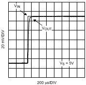 Figure 63. Step Response
8.1.2 EMI Suppression
The near-ubiquity of cellular, Bluetooth, and Wi-Fi signals and the rapid rise of sensing systems incorporating wireless radios make electromagnetic interference (EMI) an evermore important design consideration for precision signal paths. Though RF signals lie outside the op amp band, RF carrier switching can modulate the DC offset of the op amp. Also some common RF modulation schemes can induce down-converted components. The added DC offset and the induced signals are amplified with the signal of interest and thus corrupt the measurement. The LPV521 uses on chip filters to reject these unwanted RF signals at the inputs and power supply pins; thereby preserving the integrity of the precision signal path.
Twisted pair cabling and the active front-end’s common-mode rejection provide immunity against low-frequency noise (i.e. 60-Hz or 50-Hz mains) but are ineffective against RF interference. Even a few centimeters of PCB trace and wiring for sensors located close to the amplifier can pick up significant 1 GHz RF. The integrated EMI filters of the LPV521 reduce or eliminate external shielding and filtering requirements, thereby increasing system robustness. A larger EMIRR means more rejection of the RF interference. For more information on EMIRR, please refer to AN-1698.
8.2 Typical Applications
8.2.1 60-Hz Twin T-Notch Filter
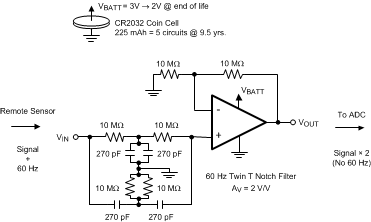 Figure 64. 60-Hz Notch Filter
8.2.1.1 Design Requirements
Small signals from transducers in remote and distributed sensing applications commonly suffer strong 60-Hz interference from AC power lines. The circuit of Figure 64 notches out the 60 Hz and provides a gain AV = 2 for the sensor signal represented by a 1-kHz sine wave. Similar stages may be cascaded to remove 2nd and 3rd harmonics of 60 Hz. Thanks to the nA power consumption of the LPV521, even 5 such circuits can run for 9.5 years from a small CR2032 lithium cell. These batteries have a nominal voltage of 3 V and an end of life voltage of 2 V. With an operating voltage from 1.6 V to 5.5 V the LPV521 can function over this voltage range.
8.2.1.2 Detailed Design Procedure
The notch frequency is set by F0 = 1 / 2πRC. To achieve a 60-Hz notch use R = 10 MΩ and C = 270 pF. If eliminating 50-Hz noise, which is common in European systems, use R = 11.8 MΩ and C = 270 pF.
The Twin T Notch Filter works by having two separate paths from VIN to the amplifier’s input. A low frequency path through the resistors R - R and another separate high frequency path through the capacitors C - C. However, at frequencies around the notch frequency, the two paths have opposing phase angles and the two signals will tend to cancel at the amplifier’s input.
To ensure that the target center frequency is achieved and to maximize the notch depth (Q factor) the filter needs to be as balanced as possible. To obtain circuit balance, while overcoming limitations of available standard resistor and capacitor values, use passives in parallel to achieve the 2C and R/2 circuit requirements for the filter components that connect to ground.
To make sure passive component values stay as expected clean board with alcohol, rinse with deionized water, and air dry. Make sure board remains in a relatively low humidity environment to minimize moisture which may increase the conductivity of board components. Also large resistors come with considerable parasitic stray capacitance which effects can be reduced by cutting out the ground plane below components of concern.
Large resistors are used in the feedback network to minimize battery drain. When designing with large resistors, resistor thermal noise, op amp current noise, as well as op amp voltage noise, must be considered in the noise analysis of the circuit. The noise analysis for the circuit in Figure 64 can be done over a bandwidth of 5 kHz, which takes the conservative approach of overestimating the bandwidth (LPV521 typical GBW/AV is lower). The total noise at the output is approximately 800 µVpp, which is excellent considering the total consumption of the circuit is only 540 nA. The dominant noise terms are op amp voltage noise (550 µVpp), current noise through the feedback network (430 µVpp), and current noise through the notch filter network (280 µVpp). Thus the total circuit's noise is below ½ LSB of a 10 bit system with a 2-V reference, which is 1 mV.
8.2.1.3 Application Curve
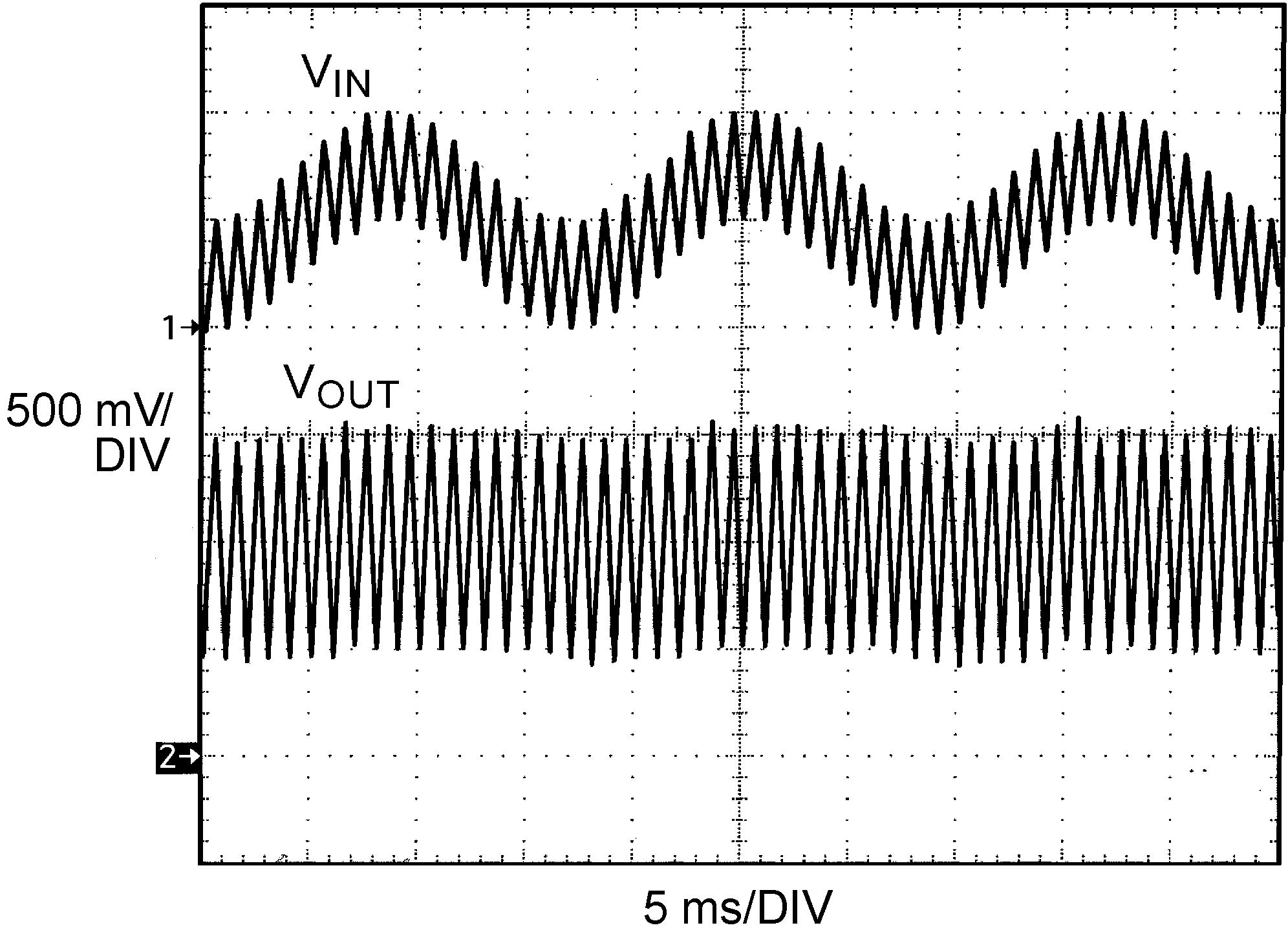 Figure 65. 60-Hz Notch Filter Waveform
8.2.2 Portable Gas Detection Sensor
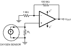 Figure 66. Precision Oxygen Sensor
8.2.2.1 Design Requirements
Gas sensors are used in many different industrial and medical applications. They generate a current which is proportional to the percentage of a particular gas sensed in an air sample. This current goes through a load resistor and the resulting voltage drop is measured. The LPV521 makes an excellent choice for this application as it only draws 345 nA of current and operates on supply voltages down to 1.6V. Depending on the sensed gas and sensitivity of the sensor, the output current can be in the order of tens of microamperes to a few milliamperes. Gas sensor datasheets often specify a recommended load resistor value or they suggest a range of load resistors to choose from.
Oxygen sensors are used when air quality or oxygen delivered to a patient needs to be monitored. Fresh air contains 20.9% oxygen. Air samples containing less than 18% oxygen are considered dangerous. This application detects oxygen in air. Oxygen sensors are also used in industrial applications where the environment must lack oxygen. An example is when food is vacuum packed. There are two main categories of oxygen sensors, those which sense oxygen when it is abundantly present (i.e. in air or near an oxygen tank) and those which detect traces of oxygen in ppm.
8.2.2.2 Detailed Design Procedure
Figure 66 shows a typical circuit used to amplify the output of an oxygen detector. The oxygen sensor outputs a known current through the load resistor. This value changes with the amount of oxygen present in the air sample. Oxygen sensors usually recommend a particular load resistor value or specify a range of acceptable values for the load resistor. The use of the nanopower LPV521 means minimal power usage by the op amp and it enhances the battery life. With the components shown in Figure 66 the circuit can consume less than 0.5 µA of current ensuring that even batteries used in compact portable electronics, with low mAh charge ratings, could last beyond the life of the oxygen sensor. The precision specifications of the LPV521, such as its very low offset voltage, low TCVOS , low input bias current, high CMRR, and high PSRR are other factors which make the LPV521 a great choice for this application.
8.2.2.3 Application Curve
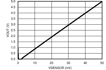 Figure 67. Calculated Oxygen Sensor Circuit Output (Single 5V Supply)
8.2.3 High-Side Battery Current Sensing
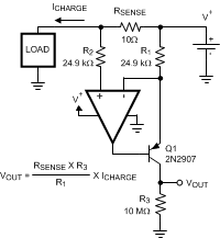 Figure 68. High-Side Current Sensing
8.2.3.1 Design Requirements
The rail-to-rail common mode input range and the very low quiescent current make the LPV521 ideal to use in high-side and low-side battery current sensing applications. The high-side current sensing circuit in Figure 68 is commonly used in a battery charger to monitor the charging current in order to prevent over charging. A sense resistor RSENSE is connected in series with the battery.
8.2.3.2 Detailed Design Procedure
The theoretical output voltage of the circuit is VOUT = [ ®SENSE × R3) / R1 ] × ICHARGE. In reality, however, due to the finite Current Gain, β, of the transistor the current that travels through R3 will not be ICHARGE, but instead, will be α × ICHARGE or β/( β+1) × ICHARGE. A Darlington pair can be used to increase the β and performance of the measuring circuit.
Using the components shown in Figure 68 will result in VOUT ≈ 4000 Ω × ICHARGE. This is ideal to amplify a 1 mA ICHARGE to near full scale of an ADC with VREF at 4.1 V. A resistor, R2 is used at the noninverting input of the amplifier, with the same value as R1 to minimize offset voltage.
Selecting values per Figure 68 will limit the current traveling through the R1 – Q1 – R3 leg of the circuit to under 1 µA which is on the same order as the LPV521 supply current. Increasing resistors R1 , R2 , and R3 will decrease the measuring circuit supply current and extend battery life.
Decreasing RSENSE will minimize error due to resistor tolerance, however, this will also decrease VSENSE = ICHARGE × RSENSE, and in turn the amplifier offset voltage will have a more significant contribution to the total error of the circuit. With the components shown in Figure 68 the measurement circuit supply current can be kept below 1.5 µA and measure 100 µA to 1 mA.
8.2.3.3 Application Curve
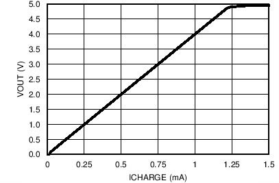 Figure 69. Calculated High-Side Current Sense Circuit Output