SNOSB14D August 2009 – December 2014 LPV521
PRODUCTION DATA.
- 1 Features
- 2 Applications
- 3 Description
- 4 Revision History
- 5 Pin Configuration and Functions
-
6 Specifications
- 6.1 Absolute Maximum Ratings
- 6.2 ESD Ratings
- 6.3 Recommended Operating Conditions
- 6.4 Thermal Information
- 6.5 1.8-V DC Electrical Characteristics
- 6.6 1.8-V AC Electrical Characteristics
- 6.7 3.3-V DC Electrical Characteristics
- 6.8 3.3-V AC Electrical Characteristics
- 6.9 5-V DC Electrical Characteristics
- 6.10 5-V AC Electrical Characteristics
- 6.11 Typical Characteristics
- 7 Detailed Description
- 8 Applications and Implementation
- 9 Power Supply Recommendations
- 10Layout
- 11Device and Documentation Support
- 12Mechanical, Packaging, and Orderable Information
Package Options
Mechanical Data (Package|Pins)
- DCK|5
Thermal pad, mechanical data (Package|Pins)
Orderable Information
6 Specifications
6.1 Absolute Maximum Ratings(1)
| MIN | MAX | UNIT | ||
|---|---|---|---|---|
| Any pin relative to V- | −0.3 | 6 | V | |
| IN+, IN-, OUT Pins | V– – 0.3 V | V+ + 0.3 V | V | |
| V+, V-, OUT Pins | 40 | mA | ||
| Differential Input Voltage (VIN+ - VIN-) | –300 | 300 | mV | |
| Junction Temperature(2) | –40 | 150 | °C | |
| Mounting Temperature | Infrared or Convection (30 sec.) | 260 | °C | |
| Wave Soldering Lead Temp. (4 sec.) | 260 | °C | ||
| Storage temperature, Tstg | −65 | 150 | °C | |
(1) indicate limits beyond which damage may occur. indicate conditions for which the device is intended to be functional, but specific performance is not guaranteed. For guaranteed specifications and test conditions, see the Electrical Characteristics.
6.2 ESD Ratings
| VALUE | UNIT | |||
|---|---|---|---|---|
| V(ESD) | Electrostatic discharge | Human-body model (HBM), per ANSI/ESDA/JEDEC JS-001(1) | ±2000 | V |
| Charged-device model (CDM), per JEDEC specification JESD22-C101(2) | ±1000 | |||
| Machine Model | ±200 | |||
(1) JEDEC document JEP155 states that 500-V HBM allows safe manufacturing with a standard ESD control process.
(2) JEDEC document JEP157 states that 250-V CDM allows safe manufacturing with a standard ESD control process.
6.3 Recommended Operating Conditions(1)
| MIN | MAX | UNIT | |
|---|---|---|---|
| Temperature Range(2) | −40 | 125 | °C |
| Supply Voltage (VS = V+ - V−) | 1.6 | 5.5 | V |
(1) indicate limits beyond which damage may occur. indicate conditions for which the device is intended to be functional, but specific performance is not guaranteed. For guaranteed specifications and test conditions, see .
6.4 Thermal Information
| THERMAL METRIC(1) | DCK | UNIT | |
|---|---|---|---|
| 5 PINS | |||
| RθJA | Junction-to-ambient thermal resistance (2) | 456 | °C/W |
(1) For more information about traditional and new thermal metrics, see the IC Package Thermal Metrics application report, SPRA953.
(2) The maximum power dissipation is a function of TJ(MAX), θJA. The maximum allowable power dissipation at any ambient temperature is PD = (TJ(MAX) – TA)/ θJA. All numbers apply for packages soldered directly onto a PC Board.
6.5 1.8-V DC Electrical Characteristics
Unless otherwise specified, all limits for TA = 25°C, V+ = 1.8 V, V− = 0 V, VCM = VO = V+/2, and RL > 1 MΩ.(1)| PARAMETER | TEST CONDITIONS | MIN | TYP | MAX | UNIT | |
|---|---|---|---|---|---|---|
| VOS | Input Offset Voltage | VCM = 0.3 V | –1 | 0.1 | 1 | mV |
| Temperature extremes | –1.23 | 1.23 | ||||
| VCM = 1.5 V | –1 | 0.1 | 1 | |||
| Temperature extremes | –1.23 | 1.23 | ||||
| TCVOS | Input Offset Voltage Drift(2) | ±0.4 | μV/°C | |||
| Temperature extremes | –3 | 3 | ||||
| IBIAS | Input Bias Current | –1 | 0.01 | 1 | pA | |
| Temperature extremes | –50 | 50 | ||||
| IOS | Input Offset Current | 10 | fA | |||
| CMRR | Common Mode Rejection Ratio | 0 V ≤ VCM ≤ 1.8 V | 66 | 92 | dB | |
| Temperature extremes | 60 | |||||
| 0 V ≤ VCM ≤ 0.7 V | 75 | 101 | ||||
| Temperature extremes | 74 | |||||
| 1.2 V ≤ VCM ≤ 1.8 V | 75 | 120 | ||||
| Temperature extremes | 53 | |||||
| PSRR | Power Supply Rejection Ratio | 1.6 V ≤ V+ ≤ 5.5 V VCM = 0.3 V |
85 |
109 | dB | |
| Temperature extremes | 76 | |||||
| CMVR | Common Mode Voltage Range | CMRR ≥ 67 dB CMRR ≥ 60 dB |
0 0 |
1.8 |
V | |
| Temperature extremes | 1.8 | |||||
| AVOL | Large Signal Voltage Gain | VO = 0.5 V to 1.3 V RL = 100 kΩ to V+/2 |
74 |
125 | dB | |
| Temperature extremes | 73 | |||||
| VO | Output Swing High | RL = 100 kΩ to V+/2 VIN(diff) = 100 mV |
2 | 50 |
mV from either rail | |
| Temperature extremes | 50 | |||||
| Output Swing Low | RL = 100 kΩ to V+/2 VIN(diff) = −100 mV |
2 | 50 |
|||
| Temperature extremes | 50 | |||||
| IO | Output Current(3) | Sourcing, VO to V–
VIN(diff) = 100 mV |
1 |
3 | mA | |
| Temperature extremes | 0.5 | |||||
| Sinking, VO to V+
VIN(diff) = −100 mV |
1 |
3 | ||||
| Temperature extremes | 0.5 | |||||
| IS | Supply Current | VCM = 0.3 V | 345 | 400 |
nA | |
| Temperature extremes | 580 | |||||
| VCM = 1.5 V | 472 | 600 |
||||
| Temperature extremes | 850 |
(1) values apply only for factory testing conditions at the temperature indicated. Factory testing conditions result in very limited self-heating of the device such that TJ = TA. No guarantee of parametric performance is indicated in the electrical tables under conditions of internal self-heating where TJ TA. indicate junction temperature limits beyond which the device may be permanently degraded, either mechanically or electrically.
(2) The offset voltage average drift is determined by dividing the change in VOS at the temperature extremes by the total temperature change.
(3) The short circuit test is a momentary open-loop test.
6.6 1.8-V AC Electrical Characteristics
Unless otherwise specified, all limits for TA = 25°C, V+ = 1.8 V, V− = 0 V, VCM = VO = V+/2, and RL > 1 MΩ.(1)| PARAMETER | TEST CONDITIONS | MIN | TYP | MAX | UNIT | ||
|---|---|---|---|---|---|---|---|
| GBW | Gain-Bandwidth Product | CL = 20 pF, RL = 100 kΩ | 6.1 | kHz | |||
| SR | Slew Rate | AV = +1, VIN = 0V to 1.8V |
Falling Edge | 2.9 | V/ms | ||
| Rising Edge | 2.3 | ||||||
| θ m | Phase Margin | CL = 20 pF, RL = 100 kΩ | 72 | deg | |||
| Gm | Gain Margin | CL = 20 pF, RL = 100 kΩ | 19 | dB | |||
| en | Input-Referred Voltage Noise Density | f = 100 Hz | 265 | nV/√Hz | |||
| Input-Referred Voltage Noise | 0.1 Hz to 10 Hz | 24 | μVPP | ||||
| In | Input-Referred Current Noise | f = 100 Hz | 100 | fA/√Hz | |||
(1) values apply only for factory testing conditions at the temperature indicated. Factory testing conditions result in very limited self-heating of the device such that TJ = TA. No guarantee of parametric performance is indicated in the electrical tables under conditions of internal self-heating where TJ TA. indicate junction temperature limits beyond which the device may be permanently degraded, either mechanically or electrically.
6.7 3.3-V DC Electrical Characteristics
Unless otherwise specified, all limits for TA = 25°C, V+ = 3.3 V, V− = 0 V, VCM = VO = V+/2, and RL > 1 MΩ.(1)| PARAMETER | TEST CONDITIONS | MIN | TYP | MAX | UNIT | |
|---|---|---|---|---|---|---|
| VOS | Input Offset Voltage | VCM = 0.3 V | –1 | 0.1 | 1 | mV |
| Temperature extremes | –1.23 | 1.23 | ||||
| VCM = 3 V | –1 | 0.1 | 1 | |||
| Temperature extremes | –1.23 | 1.23 | ||||
| TCVOS | Input Offset Voltage Drift(2) | ±0.4 | μV/°C | |||
| Temperature extremes | –3 | 3 | ||||
| IBIAS | Input Bias Current | –1 | 0.01 | 1 | pA | |
| Temperature extremes | –50 | 50 | ||||
| IOS | Input Offset Current | 20 | fA | |||
| CMRR | Common Mode Rejection Ratio | 0 V ≤ VCM ≤ 3.3 V | 72 |
97 | dB | |
| Temperature extremes | 70 | |||||
| 0 V ≤ VCM ≤ 2.2 V | 78 |
106 | ||||
| Temperature extremes | 75 | |||||
| 2.7 V ≤ VCM ≤ 3.3 V | 77 |
121 | ||||
| Temperature extremes | 76 | |||||
| PSRR | Power Supply Rejection Ratio | 1.6 V ≤ V+ ≤ 5.5 V VCM = 0.3 V |
85 |
109 | dB | |
| Temperature extremes | 76 | |||||
| CMVR | Common Mode Voltage Range | CMRR ≥ 72 dB CMRR ≥ 70 dB |
−0.1 |
3.4 |
V | |
| Temperature extremes | 0 | 3.3 | ||||
| AVOL | Large Signal Voltage Gain | VO = 0.5 V to 2.8 V RL = 100 kΩ to V+/2 |
82 |
120 | dB | |
| Temperature extremes | 76 | |||||
| VO | Output Swing High | RL = 100 kΩ to V+/2 VIN(diff) = 100 mV |
3 | 50 |
mV from either rail |
|
| Temperature extremes | 50 | |||||
| Output Swing Low | RL = 100 kΩ to V+/2 VIN(diff) = −100 mV |
2 | 50 |
|||
| Temperature extremes | 50 | |||||
| IO | Output Current(3) | Sourcing, VO to V–
VIN(diff) = 100 mV |
5 |
11 | mA | |
| Temperature extremes | 4 | |||||
| Sinking, VO to V+
VIN(diff) = −100 mV |
5 |
12 | ||||
| Temperature extremes | 4 | |||||
| IS | Supply Current | VCM = 0.3 V | 346 | 400 |
nA | |
| Temperature extremes | 600 | |||||
| VCM = 3 V | 471 | 600 |
||||
| Temperature extremes | 860 |
(1) values apply only for factory testing conditions at the temperature indicated. Factory testing conditions result in very limited self-heating of the device such that TJ = TA. No guarantee of parametric performance is indicated in the electrical tables under conditions of internal self-heating where TJ TA. indicate junction temperature limits beyond which the device may be permanently degraded, either mechanically or electrically.
(2) The offset voltage average drift is determined by dividing the change in VOS at the temperature extremes by the total temperature change.
6.8 3.3-V AC Electrical Characteristics
Unless otherwise is specified, all limits for TA = 25°C, V+ = 3.3 V, V− = 0 V, VCM = VO = V+/2, and RL > 1 MΩ.(1)| PARAMETER | TEST CONDITIONS | MIN | TYP | MAX | UNIT | ||
|---|---|---|---|---|---|---|---|
| GBW | Gain-Bandwidth Product | CL = 20 pF, RL = 100 kΩ | 6.2 | kHz | |||
| SR | Slew Rate | AV = +1, VIN = 0V to 3.3V |
Falling Edge | 2.9 | V/ms | ||
| Rising Edge | 2.5 | ||||||
| θ m | Phase Margin | CL = 20 pF, RL = 10 kΩ | 73 | deg | |||
| Gm | Gain Margin | CL = 20 pF, RL = 10 kΩ | 19 | dB | |||
| en | Input-Referred Voltage Noise Density | f = 100 Hz | 259 | nV/√Hz | |||
| Input-Referred Voltage Noise | 0.1 Hz to 10 Hz | 22 | μVPP | ||||
| In | Input-Referred Current Noise | f = 100 Hz | 100 | fA/√Hz | |||
(1) values apply only for factory testing conditions at the temperature indicated. Factory testing conditions result in very limited self-heating of the device such that TJ = TA. No guarantee of parametric performance is indicated in the electrical tables under conditions of internal self-heating where TJ TA. indicate junction temperature limits beyond which the device may be permanently degraded, either mechanically or electrically.
6.9 5-V DC Electrical Characteristics
Unless otherwise specified, all limits for TA = 25°C, V+ = 5 V, V− = 0 V, VCM = VO = V+/2, and RL > 1 MΩ.(1)| PARAMETER | TEST CONDITIONS | MIN | TYP | MAX | UNIT | |
|---|---|---|---|---|---|---|
| VOS | Input Offset Voltage | VCM = 0.3 V | 0.1 | ±1 |
mV | |
| Temperature extremes | –1.23 | 1.23 | ||||
| VCM = 4.7 V | 0.1 | ±1 |
||||
| Temperature extremes | –1.23 | 1.23 | ||||
| TCVOS | Input Offset Voltage Drift(2) | ±0.4 | μV/°C | |||
| Temperature extremes | –3.5 | 3.5 | ||||
| IBIAS | Input Bias Current | 0.04 | ±1 |
pA | ||
| Temperature extremes | –50 | 50 | ||||
| IOS | Input Offset Current | 60 | fA | |||
| CMRR | Common Mode Rejection Ratio | 0 V ≤ VCM ≤ 5.0 V | 75 |
102 | dB | |
| Temperature extremes | 74 | |||||
| 0 V ≤ VCM ≤ 3.9 V | 84 |
108 | ||||
| Temperature extremes | 80 | |||||
| 77 |
115 | |||||
| Temperature extremes | 76 | |||||
| PSRR | Power Supply Rejection Ratio | 1.6 V ≤ V+ ≤ 5.5 V VCM = 0.3 V |
85 |
109 | dB | |
| Temperature extremes | 76 | |||||
| CMVR | Common Mode Voltage Range | CMRR ≥ 75 dB CMRR ≥ 74 dB |
−0.1 |
5.1 |
V | |
| Temperature extremes | 0 | 5 | ||||
| AVOL | Large Signal Voltage Gain | VO = 0.5 V to 4.5 V RL = 100 kΩ to V+/2 |
84 |
132 | dB | |
| Temperature extremes | 76 | |||||
| VO | Output Swing High | RL = 100 kΩ to V+/2 VIN(diff) = 100 mV |
3 | 50 |
mV from either rail | |
| Temperature extremes | 50 | |||||
| Output Swing Low | RL = 100 kΩ to V+/2 VIN (diff) = −100 mV |
3 | 50 |
|||
| Temperature extremes | 50 | |||||
| IO | Output Current | Sourcing, VO to V−
VIN(diff) = 100 mV |
15 |
23 | mA | |
| Temperature extremes | 8 | |||||
| Sinking, VO to V+
VIN(diff) = −100 mV |
15 |
22 | ||||
| Temperature extremes | 8 | |||||
| IS | Supply Current | VCM = 0.3 V | 351 | 400 |
nA | |
| Temperature extremes | 620 | |||||
| VCM = 4.7 V | 475 | 600 |
||||
| Temperature extremes | 870 |
(1) values apply only for factory testing conditions at the temperature indicated. Factory testing conditions result in very limited self-heating of the device such that TJ = TA. No guarantee of parametric performance is indicated in the electrical tables under conditions of internal self-heating where TJ TA. indicate junction temperature limits beyond which the device may be permanently degraded, either mechanically or electrically.
(2) The offset voltage average drift is determined by dividing the change in VOS at the temperature extremes by the total temperature change.
(3) The short circuit test is a momentary open-loop test.
6.10 5-V AC Electrical Characteristics(1)
Unless otherwise specified, all limits for TA = 25°C, V+ = 5 V, V− = 0 V, VCM = VO = V+/2, and RL > 1 MΩ.| PARAMETER | TEST CONDITIONS | MIN (2) |
TYP (3) |
MAX (2) |
UNIT | ||
|---|---|---|---|---|---|---|---|
| GBW | Gain-Bandwidth Product | CL = 20 pF, RL = 100 kΩ | 6.2 | kHz | |||
| SR | Slew Rate | AV = +1, VIN = 0 V to 5 V |
Falling Edge | 1.1 |
2.7 | V/ms | |
| Temperature extremes | 1.2 | ||||||
| Rising Edge | 1.1 |
2.4 | |||||
| Temperature extremes | 1.2 | ||||||
| θ m | Phase Margin | CL = 20 pF, RL = 100 kΩ | 73 | deg | |||
| Gm | Gain Margin | CL = 20 pF, RL = 100 kΩ | 20 | dB | |||
| en | Input-Referred Voltage Noise Density | f = 100 Hz | 255 | nV/√Hz | |||
| Input-Referred Voltage Noise | 0.1 Hz to 10 Hz | 22 | μVPP | ||||
| In | Input-Referred Current Noise | f = 100 Hz | 100 | fA/√Hz | |||
| EMIRR | EMI Rejection Ratio, IN+ and IN−(4) | VRF_PEAK = 100 mVP (−20 dBP), f = 400 MHz |
121 | dB | |||
| VRF_PEAK = 100 mVP (−20 dBP), f = 900 MHz |
121 | ||||||
| VRF_PEAK = 100 mVP (−20 dBP), f = 1800 MHz |
124 | ||||||
| VRF_PEAK = 100 mVP (−20 dBP), f = 2400 MHz |
142 | ||||||
(1) values apply only for factory testing conditions at the temperature indicated. Factory testing conditions result in very limited self-heating of the device such that TJ = TA. No guarantee of parametric performance is indicated in the electrical tables under conditions of internal self-heating where TJ TA. indicate junction temperature limits beyond which the device may be permanently degraded, either mechanically or electrically.
(2) All limits are guaranteed by testing, statistical analysis or design.
(3) Typical values represent the most likely parametric norm at the time of characterization. Actual typical values may vary over time and will also depend on the application and configuration. The typical values are not tested and are not guaranteed on shipped production material.
(4) The EMI Rejection Ratio is defined as EMIRR = 20log (VRF_PEAK/ΔVOS).
6.11 Typical Characteristics
At TJ = 25°C, unless otherwise specified.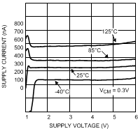 Figure 1. Supply Current vs. Supply Voltage
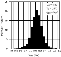 Figure 3. Offset Voltage Distribution
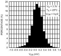 Figure 5. Offset Voltage Distribution
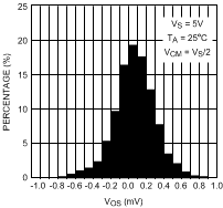 Figure 7. Offset Voltage Distribution
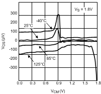 Figure 9. Input Offset Voltage vs. Input Common Mode
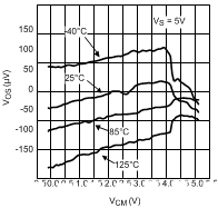 Figure 11. Input Offset Voltage vs. Input Common Mode
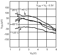 Figure 13. Input Offset Voltage vs. Supply Voltage
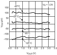 Figure 15. Input Offset Voltage vs. Output Voltage
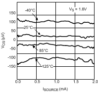 Figure 17. Input Offset Voltage vs. Sourcing Current
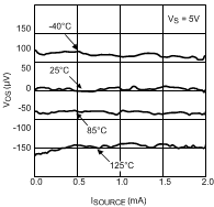 Figure 19. Input Offset Voltage vs. Sourcing Current
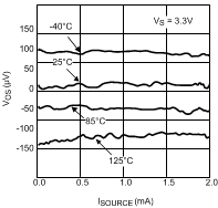 Figure 21. Input Offset Voltage vs. Sinking Current
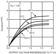 Figure 23. Sourcing Current vs. Output Voltage
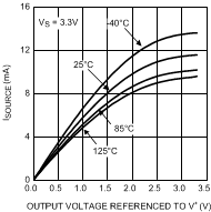 Figure 25. Sourcing Current vs. Output Voltage
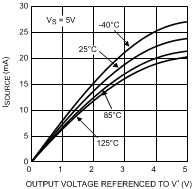 Figure 27. Sourcing Current vs. Output Voltage
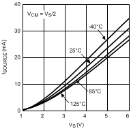 Figure 29. Sourcing Current vs. Supply Voltage
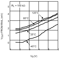 Figure 31. Output Swing High vs. Supply Voltage
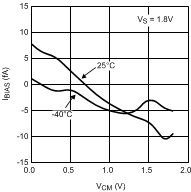 Figure 33. Input Bias Current vs. Common Mode Voltage
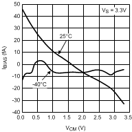 Figure 35. Input Bias Current vs. Common Mode Voltage
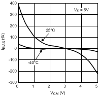 Figure 37. Input Bias Current vs. Common Mode Voltage
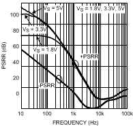 Figure 39. PSRR vs. Frequency
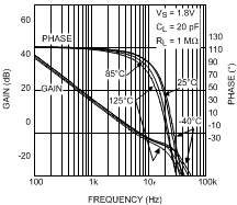 Figure 41. Frequency Response vs. Temperature
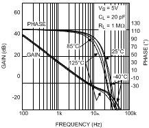 Figure 43. Frequency Response vs. Temperature
 Figure 45. Frequency Response vs. RL
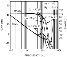 Figure 47. Frequency Response vs. CL
 Figure 49. Frequency Response vs. CL
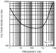 Figure 51. Voltage Noise vs. Frequency
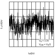 Figure 53. 0.1 to 10 Hz Time Domain Voltage Noise
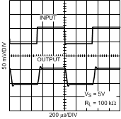 Figure 55. Small Signal Pulse Response
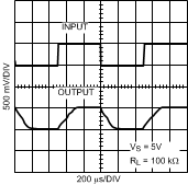 Figure 57. Large Signal Pulse Response
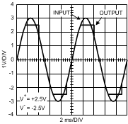
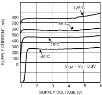 Figure 2. Supply Current vs. Supply Voltage
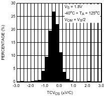 Figure 4. TcvOS Distribution
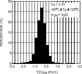 Figure 6. TcvOS Distribution
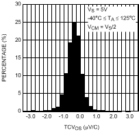 Figure 8. TcvOS Distribution
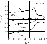 Figure 10. Input Offset Voltage vs. Input Common Mode
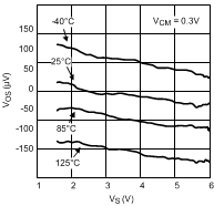 Figure 12. Input Offset Voltage vs. Supply Voltage
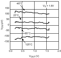 Figure 14. Input Offset Voltage vs. Output Voltage
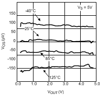 Figure 16. Input Offset Voltage vs. Output Voltage
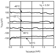 Figure 18. Input Offset Voltage vs. Sourcing Current
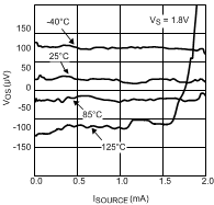 Figure 20. Input Offset Voltage vs. Sinking Current
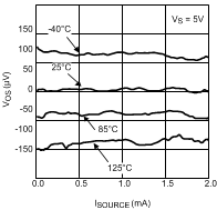 Figure 22. Input Offset Voltage vs. Sinking Current
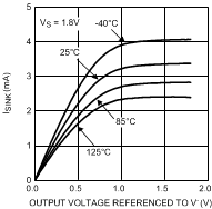 Figure 24. Sinking Current vs. Output Voltage
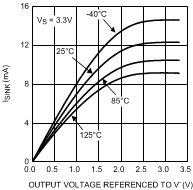 Figure 26. Sinking Current vs. Output Voltage
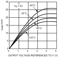 Figure 28. Sinking Current vs. Output Voltage
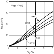 Figure 30. Sinking Current vs. Supply Voltage
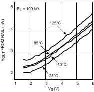 Figure 32. Output Swing Low vs. Supply Voltage
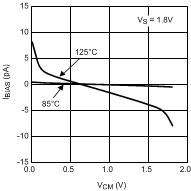 Figure 34. Input Bias Current vs. Common Mode Voltage
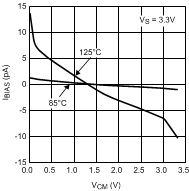 Figure 36. Input Bias Current vs. Common Mode Voltage
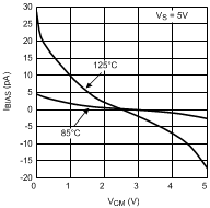 Figure 38. Input Bias Current vs. Common Mode Voltage
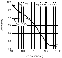 Figure 40. CMRR vs. Frequency
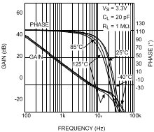 Figure 42. Frequency Response vs. Temperature
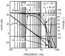 Figure 44. Frequency Response vs. RL
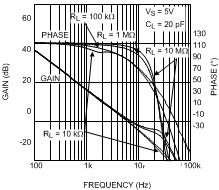 Figure 46. Frequency Response vs. RL
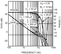 Figure 48. Frequency Response vs. CL
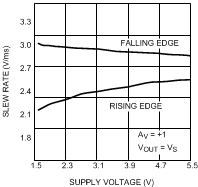 Figure 50. Slew Rate vs. Supply Voltage
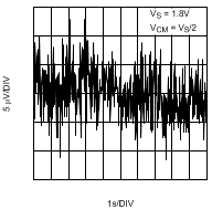 Figure 52. 0.1 to 10 Hz Time Domain Voltage Noise
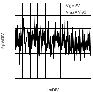 Figure 54. 0.1 to 10 Hz Time Domain Voltage Noise
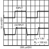 Figure 56. Small Signal Pulse Response
 Figure 58. Large Signal Pulse Response
 Figure 60. EMIRR vs. Frequency