SLLS654C April 2005 – December 2014 MC33063A-Q1
PRODUCTION DATA.
- 1 Features
- 2 Applications
- 3 Description
- 4 Revision History
- 5 Pin Configuration and Functions
- 6 Specifications
- 7 Detailed Description
- 8 Application and Implementation
- 9 Power Supply Recommendations
- 10Layout
- 11Device and Documentation Support
- 12Mechanical, Packaging, and Orderable Information
Package Options
Mechanical Data (Package|Pins)
- D|8
Thermal pad, mechanical data (Package|Pins)
Orderable Information
7 Detailed Description
7.1 Overview
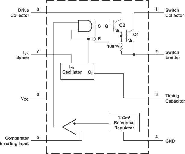
The MC33063A-Q1 device primarily consists of an internal temperature-compensated reference, a comparator, an oscillator, a PWM controller with active current limiting, a driver, and a high-current output switch. The MC33063A-Q1 device requires minimal external components to build converters in the boost, buck, and inverting topologies.
7.2 Functional Block Diagram
7.3 Feature Description
The device includes the following components:
- Temperature-compensated reference voltage
- Oscillator
- Active peak-current limit
- Output switch
- Output voltage-sense comparator
7.3.1 Reference Voltage
The reference voltage is set at 1.25 V and is used to set the output voltage of the converter.
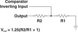 Figure 6. Reference Voltage Circuit
7.3.2 Current Limit
Current limit is accomplished by monitoring the voltage drop across an external sense resistor located in series with VCC and the output switch. The voltage drop developed across the sense resistor is monitored by the current-sense pin, Ipk. When the voltage drop across the sense resistor becomes greater than the preset value of 330 mV, the current-limit circuitry provides an additional current path to charge the timing capacitor (CT) rapidly, to reach the upper oscillator threshold and, thus, limiting the amount of energy stored in the inductor. The minimum sense resistor is 0.2 W. Figure 7 shows the timing capacitor charge current versus current-limit sense voltage. To set the peak current, Ipk = 330 mV/Rsense.
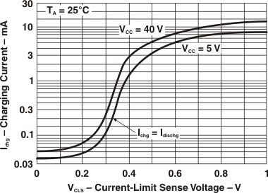 Figure 7. Timing Capacitor Charge Current vs Current-Limit Sense Voltage
7.3.3 Current Limit of Typical Operation Waveforms
The output switch is an NPN Darlington transistor. The collector of the output transistor is tied to pin 1, and the emitter is tied to pin 2. This allows the designer to use the MC33063 device in buck, boost, or inverter configurations. The maximum collector-emitter saturation voltage at 1.5 A (peak) is 1.3 V, and the maximum peak current of the output switch is 1.5 A. For higher peak output current, an external transistor can be used. Figure 8 shows the typical operation waveforms.
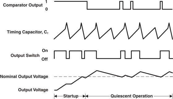 Figure 8. Typical Operation Waveforms
7.4 Device Functional Modes
The oscillator is composed of a current source and a current sink that charge and discharge the external timing capacitor (CT) between an upper and lower preset threshold. The typical charge current is 35 mA, and the typical discharge current is 200 mA, yielding approximately a 6:1 ratio. Thus, the ramp-up period is six times longer than that of the ramp-down period (see Figure 9). The upper threshold is 1.25 V, which is same as the internal reference voltage, and the lower threshold is 0.75 V. The oscillator runs constantly, at a pace controlled by the value of CT.
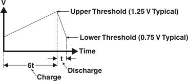 Figure 9. Oscillator Voltage Thresholds