SLAS272H July 2000 – May 2018 MSP430F133 , MSP430F135 , MSP430F147 , MSP430F1471 , MSP430F148 , MSP430F1481 , MSP430F149 , MSP430F1491
PRODUCTION DATA.
- 1Device Overview
- 2Revision History
- 3Device Comparison
- 4Terminal Configuration and Functions
-
5Specifications
- 5.1 Absolute Maximum Ratings
- 5.2 ESD Ratings
- 5.3 Recommended Operating Conditions
- 5.4 Supply Current Into AVCC and DVCC Excluding External Current
- 5.5 Thermal Resistance Characteristics
- 5.6 Schmitt-Trigger Inputs – Ports P1, P2, P3, P4, P5, and P6
- 5.7 Standard Inputs – RST/NMI, JTAG (TCK, TMS, TDI/TCLK, TDO/TDI)
- 5.8 Inputs – Px.y, TAx, TBx
- 5.9 Leakage Current
- 5.10 Outputs – Ports P1, P2, P3, P4, P5, and P6
- 5.11 Output Frequency
- 5.12 Typical Characteristics – Ports P1, P2, P3, P4, P5, and P6 Outputs
- 5.13 Wake-up Time From LPM3
- 5.14 RAM
- 5.15 Comparator_A
- 5.16 Typical Characteristics – Comparator_A
- 5.17 PUC and POR
- 5.18 DCO Frequency
- 5.19 DCO When Using ROSC
- 5.20 Crystal Oscillator, LFXT1
- 5.21 Crystal Oscillator, XT2
- 5.22 USART0, USART1
- 5.23 12-Bit ADC, Power Supply and Input Range Conditions
- 5.24 12-Bit ADC, External Reference
- 5.25 12-Bit ADC, Built-In Reference
- 5.26 12-Bit ADC, Timing Parameters
- 5.27 12-Bit ADC, Linearity Parameters
- 5.28 12-Bit ADC, Temperature Sensor and Built-In VMID
- 5.29 Flash Memory
- 5.30 JTAG Interface
- 5.31 JTAG Fuse
-
6Detailed Description
- 6.1 CPU
- 6.2 Instruction set
- 6.3 Operating Modes
- 6.4 Interrupt Vector Addresses
- 6.5 Bootloader (BSL)
- 6.6 JTAG Fuse Check Mode
- 6.7
Memory
- 6.7.1 Flash Memory
- 6.7.2
Special Function Registers
- Table 6-6 Interrupt Enable 1 Register Field Descriptions
- Table 6-7 Interrupt Enable 2 Register Field Descriptions
- Table 6-8 Interrupt Flag 1 Register Field Descriptions
- Table 6-9 Interrupt Flag 2 Register Field Descriptions
- Table 6-10 Module Enable 1 Bit Register Field Descriptions
- Table 6-11 Module Enable 2 Bit Register Field Descriptions
- 6.8
Peripherals
- 6.8.1 Digital I/O
- 6.8.2 Oscillator and System Clock
- 6.8.3 Watchdog Timer (WDT)
- 6.8.4 Hardware Multiplier (MSP430F14x and MSP430F14x1 Only)
- 6.8.5 USART0
- 6.8.6 USART1 (MSP430F14x and MSP430F14x1 Only)
- 6.8.7 Comparator_A
- 6.8.8 ADC12 (MSP430F14x and MSP430F13x Only)
- 6.8.9 Timer_A3
- 6.8.10 Timer_B3 (MSP430F13x Only)
- 6.8.11 Timer_B7 (MSP430F14x and MSP430F14x1 Only)
- 6.8.12 Peripheral File Map
- 6.9
Input/Output Diagrams
- 6.9.1 Port P1, Input/Output With Schmitt Trigger
- 6.9.2 Port P2, Input/Output With Schmitt Trigger
- 6.9.3 Port P3, Input/Output With Schmitt Trigger
- 6.9.4 Port P4, Input/Output With Schmitt Trigger
- 6.9.5 Port P5, Input/Output With Schmitt Trigger
- 6.9.6 Port P6, Input/Output With Schmitt Trigger
- 6.9.7 Port JTAG (TMS, TCK, TDI/TCLK, TDO/TDI), Input/Output With Schmitt Trigger
- 7Device and Documentation Support
- 8Mechanical, Packaging, and Orderable Information
Package Options
Mechanical Data (Package|Pins)
Thermal pad, mechanical data (Package|Pins)
- RTD|64
Orderable Information
5.25 12-Bit ADC, Built-In Reference
over recommended operating supply voltage and free-air temperature (unless otherwise noted)| PARAMETER | TEST CONDITIONS | VCC | MIN | TYP | MAX | UNIT | |
|---|---|---|---|---|---|---|---|
| VREF+ | Positive built-in reference voltage output | REF2_5V = 1 for 2.5 V,
IVREF+ ≤ IVREF+(max) |
3 V | 2.4 | 2.5 | 2.6 | V |
| REF2_5V = 0 for 1.5 V,
IVREF+ ≤ IVREF+(max) |
2.2 V, 3 V | 1.44 | 1.5 | 1.56 | |||
| AVCC(min) | AVCC minimum voltage, positive built-in reference active | REF2_5V = 0, IVREF+ ≤ 1 mA | 2.2 | V | |||
| REF2_5V = 1, IVREF+ ≤ 0.5 mA | VREF+ + 0.15 | ||||||
| REF2_5V = 1, IVREF+ ≤ 1 mA | VREF+ + 0.15 | ||||||
| IVREF+ | Load current out of VREF+ terminal | 2.2 V | 0.01 | –0.5 | mA | ||
| 3 V | –1 | ||||||
| IL(VREF)+ | Load-current regulation, VREF+ terminal(3) | IVREF+ = 500 µA ±100 µA,
Analog input voltage ≈ 0.75 V, REF2_5V = 0 |
2.2 V | ±2 | LSB | ||
| 3 V | ±2 | ||||||
| IVREF+ = 500 µA ±100 µA,
Analog input voltage ≈ 1.25 V, REF2_5V = 1 |
3 V | ±2 | LSB | ||||
| IDL(VREF)+ | Load-current regulation, VREF+ terminal(4) | IVREF+ = 100 µA to 90 µA,
CVREF+ = 5 µF, VAx ≈ 0 5 × VREF+, Error of conversion result ≤ 1 LSB |
3 V | 20 | ns | ||
| CVREF+ | Capacitance at VREF+ terminal(1) | REFON = 1,
0 mA ≤ IVREF+ ≤ IVREF+(max) |
2.2 V, 3 V | 5 | 10 | µF | |
| TREF+ | Temperature coefficient of built-in reference(3) |
IVREF+ is constant in the range of 0 mA ≤ IVREF+ ≤ 1 mA |
2.2 V, 3 V | ±100 | ppm/°C | ||
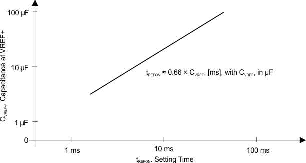
| tREFON | Settling time of reference voltage(2)(3) (see Figure 5-13) | IVREF+ = 0.5 mA, CVREF+ = 10 µF,
VVREF+ = 1.5 V, VAVCC = 2.2 V |
17 | ms | |||
(1) The internal buffer operational amplifier and the accuracy specifications require an external capacitor. All INL and DNL tests uses two capacitors between pins VREF+ and AVSS and VREF−/VeREF− and AVSS: 10-µF tantalum and 100-nF ceramic.
(2) The condition is that the error in a conversion started after tREFON is less than ±0.5 LSB. The settling time depends on the external capacitive load.
(3) Not production tested, limits characterized
(4) Not production tested, limits verified by design
 Figure 5-13 Typical Settling Time of Internal Reference (tREFON) vs External Capacitor on VREF+
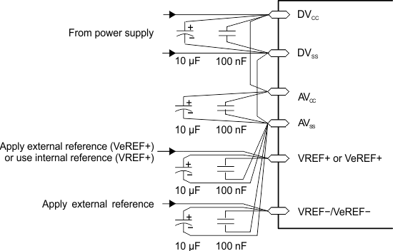
 Figure 5-14 Supply Voltage and Reference Voltage Design, VREF−/VeREF− External Supply
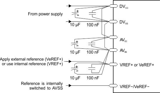
 Figure 5-15 Supply Voltage and Reference Voltage Design, VREF-/VeREF- = AVSS, Internally Connected