SLAS541M June 2007 – March 2022 MSP430F2416 , MSP430F2417 , MSP430F2418 , MSP430F2419 , MSP430F2616 , MSP430F2617 , MSP430F2618 , MSP430F2619
PRODUCTION DATA
- 1 Features
- 2 Applications
- 3 Description
- 4 Functional Block Diagrams
- 5 Revision History
- 6 Device Comparison
- 7 Terminal Configuration and Functions
-
8 Specifications
- 8.1 Absolute Maximum Ratings
- 8.2 ESD Ratings
- 8.3 Recommended Operating Conditions
- 8.4 Active Mode Supply Current Into VCC Excluding External Current
- 8.5 Typical Characteristics – Active Mode Supply Current (Into VCC)
- 8.6 Low-Power Mode Supply Currents (Into VCC) Excluding External Current
- 8.7 Typical Characteristics – LPM4 Current
- 8.8 Schmitt-Trigger Inputs (Ports P1 to P8, RST/NMI, JTAG, XIN, and XT2IN)
- 8.9 Inputs (Ports P1 and P2)
- 8.10 Leakage Current (Ports P1 to P8)
- 8.11 Standard Inputs ( RST/NMI)
- 8.12 Outputs (Ports P1 to P8)
- 8.13 Output Frequency (Ports P1 to P8)
- 8.14 Typical Characteristics – Outputs
- 8.15 POR and Brownout Reset (BOR)
- 8.16 Typical Characteristics – POR and BOR
- 8.17 Supply Voltage Supervisor (SVS), Supply Voltage Monitor (SVM)
- 8.18 Main DCO Characteristics
- 8.19 DCO Frequency
- 8.20 Calibrated DCO Frequencies – Tolerance at Calibration
- 8.21 Calibrated DCO Frequencies – Tolerance Over Temperature 0°C to 85°C
- 8.22 Calibrated DCO Frequencies – Tolerance Over Supply Voltage VCC
- 8.23 Calibrated DCO Frequencies – Overall Tolerance
- 8.24 Typical Characteristics – Calibrated DCO Frequency
- 8.25 Wake-up Times From Lower-Power Modes (LPM3, LPM4)
- 8.26 Typical Characteristics – DCO Clock Wake-up Time From LPM3 or LPM4
- 8.27 DCO With External Resistor ROSC
- 8.28 Typical Characteristics – DCO With External Resistor ROSC
- 8.29 Crystal Oscillator LFXT1, Low-Frequency Mode
- 8.30 Internal Very-Low-Power Low-Frequency Oscillator (VLO)
- 8.31 Crystal Oscillator LFXT1, High-Frequency Mode
- 8.32 Typical Characteristics – LFXT1 Oscillator in HF Mode (XTS = 1)
- 8.33 Crystal Oscillator XT2
- 8.34 Typical Characteristics – XT2 Oscillator
- 8.35 Timer_A
- 8.36 Timer_B
- 8.37 USCI (UART Mode)
- 8.38 USCI (SPI Master Mode)
- 8.39 USCI (SPI Slave Mode)
- 8.40 USCI (I2C Mode)
- 8.41 Comparator_A+
- 8.42 Typical Characteristics – Comparator_A+
- 8.43 12-Bit ADC Power Supply and Input Range Conditions
- 8.44 12-Bit ADC External Reference
- 8.45 12-Bit ADC Built-In Reference
- 8.46 12-Bit ADC Timing Parameters
- 8.47 12-Bit ADC Linearity Parameters
- 8.48 12-Bit ADC Temperature Sensor and Built-In VMID
- 8.49 12-Bit DAC Supply Specifications
- 8.50 12-Bit DAC Linearity Specifications
- 8.51 Typical Characteristics, 12-Bit DAC Linearity Specifications
- 8.52 12-Bit DAC Output Specifications
- 8.53 12-Bit DAC Reference Input Specifications
- 8.54 12-Bit DAC Dynamic Specifications
- 8.55 Flash Memory
- 8.56 RAM
- 8.57 JTAG Interface
- 8.58 JTAG Fuse
-
9 Detailed Description
- 9.1 CPU
- 9.2 Instruction Set
- 9.3 Operating Modes
- 9.4 Interrupt Vector Addresses
- 9.5 Special Function Registers (SFRs)
- 9.6 Memory Organization
- 9.7 Bootloader (BSL)
- 9.8 Flash Memory
- 9.9
Peripherals
- 9.9.1 DMA Controller (MSP430F261x Only)
- 9.9.2 Oscillator and System Clock
- 9.9.3 Calibration Data Stored in Information Memory Segment A
- 9.9.4 Brownout, Supply Voltage Supervisor (SVS)
- 9.9.5 Digital I/O
- 9.9.6 Watchdog Timer (WDT+)
- 9.9.7 Hardware Multiplier
- 9.9.8 Universal Serial Communication Interface (USCI)
- 9.9.9 Timer_A3
- 9.9.10 Timer_B7
- 9.9.11 Comparator_A+
- 9.9.12 ADC12
- 9.9.13 DAC12 (MSP430F261x Only)
- 9.9.14 Peripheral File Map
- 9.10
Port Diagrams
- 9.10.1 Port P1 (P1.0 to P1.7), Input/Output With Schmitt Trigger
- 9.10.2 Port P2 (P2.0 to P2.4, P2.6, and P2.7), Input/Output With Schmitt Trigger
- 9.10.3 Port P2 (P2.5), Input/Output With Schmitt Trigger
- 9.10.4 Port P3 (P3.0 to P3.7), Input/Output With Schmitt Trigger
- 9.10.5 Port P4 (P4.0 to P4.7), Input/Output With Schmitt Trigger
- 9.10.6 Port P5 (P5.0 to P5.7), Input/Output With Schmitt Trigger
- 9.10.7 Port P6 (P6.0 to P6.4), Input/Output With Schmitt Trigger
- 9.10.8 Port P6 (P6.5 and P6.6), Input/Output With Schmitt Trigger
- 9.10.9 Port P6 (P6.7), Input/Output With Schmitt Trigger
- 9.10.10 Port P7 (P7.0 to P7.7), Input/Output With Schmitt Trigger
- 9.10.11 Port P8 (P8.0 to P8.5), Input/Output With Schmitt Trigger
- 9.10.12 Port P8 (P8.6), Input/Output With Schmitt Trigger
- 9.10.13 Port P8 (P8.7), Input/Output With Schmitt Trigger
- 9.10.14 JTAG Pins (TMS, TCK, TDI/TCLK, TDO/TDI) Input/Output With Schmitt Trigger
- 9.10.15 JTAG Fuse Check Mode
- 10Device and Documentation Support
- 11Mechanical, Packaging, and Orderable Information
Package Options
Mechanical Data (Package|Pins)
Thermal pad, mechanical data (Package|Pins)
Orderable Information
8.45 12-Bit ADC Built-In Reference
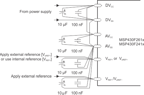
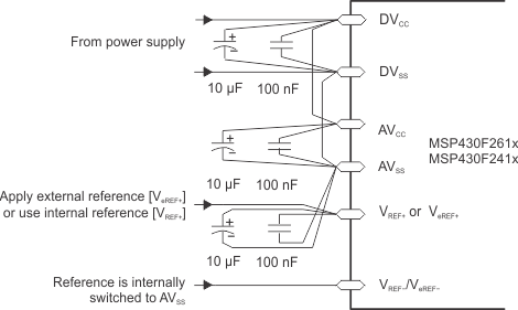
over recommended operating free-air temperature range (unless otherwise noted) (see Figure 8-39 and Figure 8-40)
| PARAMETER | TEST CONDITIONS | TA | VCC | MIN | TYP | MAX | UNIT | |
|---|---|---|---|---|---|---|---|---|
| VREF+ | Positive built-in reference voltage output | REF2_5V = 1 for 2.5 V, IVREF+max ≤ IVREF+ ≤ IVREF+min |
–40°C to 85°C | 3 V | 2.4 | 2.5 | 2.6 | V |
| 105°C | 2.37 | 2.5 | 2.64 | |||||
| REF2_5V = 0 for 1.5 V, IVREF+max ≤ IVREF+ ≤ IVREF+min |
–40°C to 85°C | 2.2 V, 3 V | 1.44 | 1.5 | 1.56 | |||
| 105°C | 1.42 | 1.5 | 1.57 | |||||
| AVCC(min) | AVCC minimum voltage, positive built-in reference active | REF2_5V = 0, IVREF+max ≤ IVREF+ ≤ IVREF+min |
2.2 | V | ||||
| REF2_5V = 1, –0.5 mA ≤ IVREF+ ≤ IVREF+min |
2.8 | |||||||
| REF2_5V = 1, –1 mA ≤ IVREF+ ≤ IVREF+min |
2.9 | |||||||
| IVREF+ | Load current out of VREF+terminal | 2.2 V | 0.01 | –0.5 | mA | |||
| 3 V | 0.01 | –1 | ||||||
| IL(VREF)+ | Load-current regulation, VREF+ terminal (1) | IVREF+ = 500 µA ±100 µA, Analog input voltage ≈ 0.75 V, REF2_5V = 0 |
2.2 V | ±2 | LSB | |||
| 3 V | ±2 | |||||||
| IVREF+ = 500 µA ±100 µA, Analog input voltage ≈ 1.25 V, REF2_5V = 1 |
3 V | ±2 | ||||||
| IDL(VREF) + | Load current regulation, VREF+ terminal (2) | IVREF+ = 100 µA → 900 µA, CVREF+ = 5 µF, Ax ≈ 0.5 × VREF+, Error of conversion result ≤ 1 LSB |
3 V | 20 | ns | |||
| CVREF+ | Capacitance at pin VREF+(3) | REFON = 1, 0 mA ≤ IVREF+ ≤ IVREF+max |
2.2 V, 3 V | 5 | 10 | µF | ||
| TREF+ | Temperature coefficient of built-in reference (2) | IVREF+ is a constant in the range of 0 mA ≤ IVREF+ ≤ 1 mA |
2.2 V, 3 V | ±100 | ppm/°C | |||
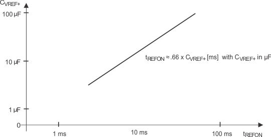
| tREFON | Settling time of internal reference voltage (see Figure 8-38)(2)(4) | IVREF+ = 0.5 mA, CVREF+ = 10 µF, VREF+ = 1.5 V, VAVCC = 2.2 V |
2.2 V | 17 | ms | |||
(1) Not production tested, limits characterized
(2) Not production tested, limits verified by design
(3) The internal buffer operational amplifier and the accuracy specifications require an external capacitor. All INL and DNL
tests use two capacitors between pins VREF+ and AVSS and between VREF-/VeREF- and
AVSS: 10-µF tantalum and 100-nF ceramic.
(4) The condition is that the error in a conversion started after tREFON is less than ±0.5 LSB. The settling time
depends on the external capacitive load.
 Figure 8-38 Typical Settling Time of Internal Reference tREFON vs
External Capacitor on VREF+
 Figure 8-39 Supply Voltage and Reference Voltage Design
VREF-/VeREF- External Supply
 Figure 8-40 Supply Voltage and Reference Voltage Design
VREF-/VeREF- = AVSS, Internally Connected