SLAS612F August 2009 – September 2018 MSP430F5418 , MSP430F5419 , MSP430F5435 , MSP430F5436 , MSP430F5437 , MSP430F5438
PRODUCTION DATA.
- 1Device Overview
- 2Revision History
- 3Device Comparison
- 4Terminal Configuration and Functions
-
5Specifications
- 5.1 Absolute Maximum Ratings
- 5.2 ESD Ratings
- 5.3 Recommended Operating Conditions
- 5.4 Active Mode Supply Current Into VCC Excluding External Current
- 5.5 Low-Power Mode Supply Currents (Into VCC) Excluding External Current
- 5.6 Thermal Resistance Characteristics
- 5.7 Schmitt-Trigger Inputs – General-Purpose I/O
- 5.8 Inputs – Ports P1 and P2
- 5.9 Leakage Current – General-Purpose I/O
- 5.10 Outputs – General-Purpose I/O (Full Drive Strength)
- 5.11 Outputs – General-Purpose I/O (Reduced Drive Strength)
- 5.12 Output Frequency – General-Purpose I/O
- 5.13 Typical Characteristics – Outputs, Reduced Drive Strength (PxDS.y = 0)
- 5.14 Typical Characteristics – Outputs, Full Drive Strength (PxDS.y = 1)
- 5.15 Crystal Oscillator, XT1, Low-Frequency Mode
- 5.16 Crystal Oscillator, XT1, High-Frequency Mode
- 5.17 Crystal Oscillator, XT2
- 5.18 Internal Very-Low-Power Low-Frequency Oscillator (VLO)
- 5.19 Internal Reference, Low-Frequency Oscillator (REFO)
- 5.20 DCO Frequency
- 5.21 PMM, Brownout Reset (BOR)
- 5.22 PMM, Core Voltage
- 5.23 PMM, SVS High Side
- 5.24 PMM, SVM High Side
- 5.25 PMM, SVS Low Side
- 5.26 PMM, SVM Low Side
- 5.27 Wake-up Times From Low-Power Modes
- 5.28 Timer_A
- 5.29 Timer_B
- 5.30 USCI (UART Mode) Clock Frequency
- 5.31 USCI (UART Mode)
- 5.32 USCI (SPI Master Mode) Clock Frequency
- 5.33 USCI (SPI Master Mode)
- 5.34 USCI (SPI Slave Mode)
- 5.35 USCI (I2C Mode)
- 5.36 12-Bit ADC, Power Supply and Input Range Conditions
- 5.37 12-Bit ADC, External Reference
- 5.38 12-Bit ADC, Built-In Reference
- 5.39 12-Bit ADC, Timing Parameters
- 5.40 12-Bit ADC, Linearity Parameters
- 5.41 12-Bit ADC, Temperature Sensor and Built-In VMID
- 5.42 Flash Memory
- 5.43 JTAG and Spy-Bi-Wire Interface
-
6Detailed Description
- 6.1 CPU
- 6.2 Operating Modes
- 6.3 Interrupt Vector Addresses
- 6.4 Memory Organization
- 6.5 Bootloader (BSL)
- 6.6 JTAG Operation
- 6.7 Flash Memory (Link to User's Guide)
- 6.8 RAM (Link to User's Guide)
- 6.9
Peripherals
- 6.9.1 Digital I/O (Link to User's Guide)
- 6.9.2 Oscillator and System Clock (Link to User's Guide)
- 6.9.3 Power-Management Module (PMM) (Link to User's Guide)
- 6.9.4 Hardware Multiplier (Link to User's Guide)
- 6.9.5 Real-Time Clock (RTC_A) (Link to User's Guide)
- 6.9.6 Watchdog Timer (WDT_A) (Link to User's Guide)
- 6.9.7 System Module (SYS) (Link to User's Guide)
- 6.9.8 DMA Controller (Link to User's Guide)
- 6.9.9 Universal Serial Communication Interface (USCI) (Links to User's Guide: UART Mode, SPI Mode, I2C Mode)
- 6.9.10 TA0 (Link to User's Guide)
- 6.9.11 TA1 (Link to User's Guide)
- 6.9.12 TB0 (Link to User's Guide)
- 6.9.13 ADC12_A (Link to User's Guide)
- 6.9.14 CRC16 (Link to User's Guide)
- 6.9.15 Embedded Emulation Module (EEM) (L Version) (Link to User's Guide)
- 6.9.16 Peripheral File Map
- 6.10
Input/Output Diagrams
- 6.10.1 Port P1, P1.0 to P1.7, Input/Output With Schmitt Trigger
- 6.10.2 Port P2, P2.0 to P2.7, Input/Output With Schmitt Trigger
- 6.10.3 Port P3, P3.0 to P3.7, Input/Output With Schmitt Trigger
- 6.10.4 Port P4, P4.0 to P4.7, Input/Output With Schmitt Trigger
- 6.10.5 Port P5, P5.0 and P5.1, Input/Output With Schmitt Trigger
- 6.10.6 Port P5, P5.2, Input/Output With Schmitt Trigger
- 6.10.7 Port P5, P5.3, Input/Output With Schmitt Trigger
- 6.10.8 Port P5, P5.4 to P5.7, Input/Output With Schmitt Trigger
- 6.10.9 Port P6, P6.0 to P6.7, Input/Output With Schmitt Trigger
- 6.10.10 Port P7, P7.0, Input/Output With Schmitt Trigger
- 6.10.11 Port P7, P7.1, Input/Output With Schmitt Trigger
- 6.10.12 Port P7, P7.2 and P7.3, Input/Output With Schmitt Trigger
- 6.10.13 Port P7, P7.4 to P7.7, Input/Output With Schmitt Trigger
- 6.10.14 Port P8, P8.0 to P8.7, Input/Output With Schmitt Trigger
- 6.10.15 Port P9, P9.0 to P9.7, Input/Output With Schmitt Trigger
- 6.10.16 Port P10, P10.0 to P10.7, Input/Output With Schmitt Trigger
- 6.10.17 Port P11, P11.0 to P11.2, Input/Output With Schmitt Trigger
- 6.10.18 Port J, J.0 JTAG Pin TDO, Input/Output With Schmitt Trigger or Output
- 6.10.19 Port J, J.1 to J.3 JTAG Pins TMS, TCK, TDI/TCLK, Input/Output With Schmitt Trigger or Output
- 6.11 TLV (Device Descriptor) Structures
- 7Device and Documentation Support
- 8Mechanical, Packaging, and Orderable Information
Package Options
Mechanical Data (Package|Pins)
- PN|80
Thermal pad, mechanical data (Package|Pins)
Orderable Information
7.2 Device Nomenclature
To designate the stages in the product development cycle, TI assigns prefixes to the part numbers of all MSP MCU devices. Each MSP MCU commercial family member has one of two prefixes: MSP or XMS. These prefixes represent evolutionary stages of product development from engineering prototypes (XMS) through fully qualified production devices (MSP).
XMS – Experimental device that is not necessarily representative of the final device's electrical specifications
MSP – Fully qualified production device
XMS devices are shipped against the following disclaimer:
"Developmental product is intended for internal evaluation purposes."
MSP devices have been characterized fully, and the quality and reliability of the device have been demonstrated fully. TI's standard warranty applies.
Predictions show that prototype devices (XMS) have a greater failure rate than the standard production devices. TI recommends that these devices not be used in any production system because their expected end-use failure rate still is undefined. Only qualified production devices are to be used.
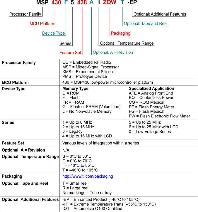
TI device nomenclature also includes a suffix with the device family name. This suffix indicates the temperature range, package type, and distribution format. Figure 7-1 provides a legend for reading the complete device name.
 Figure 7-1 Device Nomenclature