SLAS580E October 2008 – May 2020 MSP430FG477 , MSP430FG478 , MSP430FG479
PRODUCTION DATA.
- 1Device Overview
- 2Revision History
- 3Device Comparison
- 4Terminal Configuration and Functions
-
5Specifications
- 5.1 Absolute Maximum Ratings
- 5.2 ESD Ratings
- 5.3 Recommended Operating Conditions
- 5.4 Supply Current Into AVCC and DVCC Excluding External Current
- 5.5 Schmitt-Trigger Inputs – Ports P1 to P6, RST/NMI, JTAG (TCK, TMS, TDI/TCLK,TDO/TDI)
- 5.6 Inputs Px.y, TAx
- 5.7 Leakage Current – Ports P1 to P6
- 5.8 Outputs – Ports P1 to P6
- 5.9 Output Frequency
- 5.10 Typical Characteristics – Outputs
- 5.11 Wake-up Timing From LPM3
- 5.12 POR – Brownout Reset (BOR)
- 5.13 SVS (Supply Voltage Supervisor and Monitor)
- 5.14 DCO
- 5.15 Crystal Oscillator, LFXT1, Low-Frequency Mode
- 5.16 Crystal Oscillator, LFXT1, High-Frequency Mode
- 5.17 Crystal Oscillator, XT2 Oscillator, High-Frequency Mode
- 5.18 RAM
- 5.19 LCD_A
- 5.20 Comparator_A
- 5.21 Typical Characteristics – Comparator_A
- 5.22 SD16_A, Power Supply and Recommended Operating Conditions
- 5.23 SD16_A, Input Range
- 5.24 SD16_A, Performance
- 5.25 SD16_A, Performance
- 5.26 SD16_A, Linearity
- 5.27 Typical Characteristics, SD16_A SINAD Performance Over OSR
- 5.28 SD16_A, Temperature Sensor and Built-in VCC Sense
- 5.29 SD16_A, Built-In Voltage Reference
- 5.30 SD16_A, Reference Output Buffer
- 5.31 SD16_A, External Reference Input
- 5.32 12-Bit DAC, Supply Specifications
- 5.33 12-Bit DAC, Linearity Specifications
- 5.34 12-Bit DAC, Output Specifications
- 5.35 12-Bit DAC, Reference Input Specifications
- 5.36 12-Bit DAC, Dynamic Specifications
- 5.37 12-Bit DAC, Dynamic Specifications Continued
- 5.38 Operational Amplifier OA, Supply Specifications
- 5.39 Operational Amplifier OA, Input/Output Specifications
- 5.40 Operational Amplifier OA, Dynamic Specifications
- 5.41 Operational Amplifier OA, Typical Characteristics
- 5.42 Switches Between OA Terminals and Pins
- 5.43 OA Typical Characteristics
- 5.44 Timer_A
- 5.45 Timer_B
- 5.46 USCI (UART Mode)
- 5.47 USCI (SPI Master Mode)
- 5.48 USCI (SPI Slave Mode)
- 5.49 USCI (I2C Mode)
- 5.50 Flash Memory
- 5.51 JTAG Interface
- 5.52 JTAG Fuse
-
6Detailed Description
- 6.1 CPU
- 6.2 Instruction Set
- 6.3 Operating Modes
- 6.4 Interrupt Vector Addresses
- 6.5 Special Function Registers (SFRs)
- 6.6 Memory Organization
- 6.7 Bootloader (BSL)
- 6.8 Flash Memory
- 6.9
Peripherals
- 6.9.1 Oscillator and System Clock
- 6.9.2 Brownout, Supply Voltage Supervisor (SVS)
- 6.9.3 Digital I/O
- 6.9.4 Watchdog Timer (WDT+)
- 6.9.5 Basic Timer1 and Real-Time Clock
- 6.9.6 LCD_A Drive With Regulated Charge Pump
- 6.9.7 Timer_A3
- 6.9.8 Timer_B3
- 6.9.9 Universal Serial Communication Interface (USCI)
- 6.9.10 Comparator_A
- 6.9.11 SD16_A
- 6.9.12 DAC12
- 6.9.13 OA
- 6.9.14 Peripheral File Map
- 6.10
Input/Output Schematics
- 6.10.1 Port P1, P1.0, Input/Output With Schmitt Trigger
- 6.10.2 Port P1, P1.1, Input/Output With Schmitt Trigger
- 6.10.3 Port P1, P1.2, Input/Output With Schmitt Trigger
- 6.10.4 Port P1, P1.3, Input/Output With Schmitt Trigger
- 6.10.5 Port P1, P1.4, Input/Output With Schmitt Trigger
- 6.10.6 Port P1, P1.5, Input/Output With Schmitt Trigger
- 6.10.7 Port P1, P1.6, Input/Output With Schmitt Trigger
- 6.10.8 Port P1, P1.7, Input/Output With Schmitt Trigger
- 6.10.9 Port P2, P2.0 and P2.1, Input/Output With Schmitt Trigger
- 6.10.10 Port P2, P2.2 and P2.3, Input/Output With Schmitt Trigger
- 6.10.11 Port P2, P2.4 and P2.5, Input/Output With Schmitt Trigger
- 6.10.12 Port P2, P2.6 and P2.7, Input/Output With Schmitt Trigger
- 6.10.13 Port P3, P3.0 and P3.3, Input/Output With Schmitt Trigger
- 6.10.14 Port P3, P3.1 and P3.2, Input/Output With Schmitt Trigger
- 6.10.15 Port P3, P3.4 to P3.7, Input/Output With Schmitt Trigger
- 6.10.16 Port P4, P4.0 to P4.7, Input/Output With Schmitt Trigger
- 6.10.17 Port P5, P5.0 and P5.1, Input/Output With Schmitt Trigger
- 6.10.18 Port P5, P5.2 to P5.7, Input/Output With Schmitt Trigger
- 6.10.19 Port P6, P6.0 and P6.3, Input/Output With Schmitt Trigger
- 6.10.20 Port P6, P6.1 and P6.4, Input/Output With Schmitt Trigger
- 6.10.21 Port P6, P6.2, P6.5, and P6.6, Input/Output With Schmitt Trigger
- 6.10.22 Port P6, P6.7, Input/Output With Schmitt Trigger
- 6.10.23 Segment Pin Schematic: Sx, Dedicated Segment Pins
- 6.10.24 Segment Pin Schematic: COM0, Dedicated COM0 Pin
- 6.10.25 JTAG Pins TMS, TCK, TDI/TCLK, TDO/TDI, Input/Output With Schmitt Trigger or Output
- 6.10.26 JTAG Fuse Check Mode
-
7Device and Documentation Support
- 7.1 Device Support
- 7.2 Documentation Support
- 7.3 Related Links
- 7.4 Support Resources
- 7.5 Trademarks
- 7.6 Electrostatic Discharge Caution
- 7.7 Export Control Notice
- 7.8 Glossary
- 8Mechanical, Packaging, and Orderable Information
Package Options
Mechanical Data (Package|Pins)
Thermal pad, mechanical data (Package|Pins)
Orderable Information
7.1.3 Device Nomenclature
To designate the stages in the product development cycle, TI assigns prefixes to the part numbers of all MSP MCU devices. Each MSP MCU commercial family member has one of two prefixes: MSP or XMS. These prefixes represent evolutionary stages of product development from engineering prototypes (XMS) through fully qualified production devices (MSP).
XMS – Experimental device that is not necessarily representative of the final device's electrical specifications
MSP – Fully qualified production device
XMS devices are shipped against the following disclaimer:
"Developmental product is intended for internal evaluation purposes."
MSP devices have been characterized fully, and the quality and reliability of the device have been demonstrated fully. TI's standard warranty applies.
Predictions show that prototype devices (XMS) have a greater failure rate than the standard production devices. TI recommends that these devices not be used in any production system because their expected end-use failure rate still is undefined. Only qualified production devices are to be used.
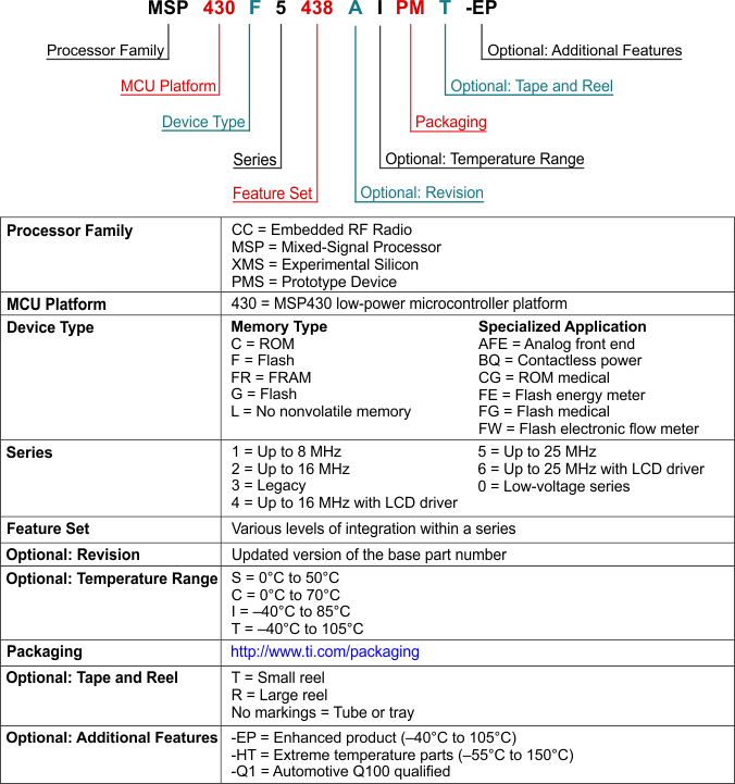
TI device nomenclature also includes a suffix with the device family name. This suffix indicates the temperature range, package type, and distribution format. Figure 7-1 provides a legend for reading the complete device name.
 Figure 7-1 Device Nomenclature