SLASE45E October 2014 – December 2019 MSP430FR2032 , MSP430FR2033
PRODUCTION DATA.
- 1Device Overview
- 2Revision History
- 3Device Comparison
- 4Terminal Configuration and Functions
-
5Specifications
- 5.1 Absolute Maximum Ratings
- 5.2 ESD Ratings
- 5.3 Recommended Operating Conditions
- 5.4 Active Mode Supply Current Into VCC Excluding External Current
- 5.5 Active Mode Supply Current Per MHz
- 5.6 Low-Power Mode LPM0 Supply Currents Into VCC Excluding External Current
- 5.7 Low-Power Mode LPM3 and LPM4 Supply Currents (Into VCC) Excluding External Current
- 5.8 Low-Power Mode LPMx.5 Supply Currents (Into VCC) Excluding External Current
- 5.9 Typical Characteristics, Low-Power Mode Supply Currents
- 5.10 Typical Characteristics - Current Consumption Per Module
- 5.11 Thermal Characteristics
- 5.12
Timing and Switching Characteristics
- 5.12.1 Power Supply Sequencing
- 5.12.2 Reset Timing
- 5.12.3 Clock Specifications
- 5.12.4 Digital I/Os
- 5.12.5 Timer_A
- 5.12.6
eUSCI
- Table 5-11 eUSCI (UART Mode) Recommended Operating Conditions
- Table 5-12 eUSCI (UART Mode) Switching Characteristics
- Table 5-13 eUSCI (SPI Master Mode) Recommended Operating Conditions
- Table 5-14 eUSCI (SPI Master Mode) Switching Characteristics
- Table 5-15 eUSCI (SPI Slave Mode) Switching Characteristics
- Table 5-16 eUSCI (I2C Mode) Switching Characteristics
- 5.12.7 ADC
- 5.12.8 FRAM
- 5.12.9 Emulation and Debug
-
6Detailed Description
- 6.1 CPU
- 6.2 Operating Modes
- 6.3 Interrupt Vector Addresses
- 6.4 Bootloader (BSL)
- 6.5 JTAG Standard Interface
- 6.6 Spy-Bi-Wire Interface (SBW)
- 6.7 FRAM
- 6.8 Memory Protection
- 6.9
Peripherals
- 6.9.1 Power Management Module (PMM) and On-chip Reference Voltages
- 6.9.2 Clock System (CS) and Clock Distribution
- 6.9.3 General-Purpose Input/Output Port (I/O)
- 6.9.4 Watchdog Timer (WDT)
- 6.9.5 System Module (SYS)
- 6.9.6 Cyclic Redundancy Check (CRC)
- 6.9.7 Enhanced Universal Serial Communication Interface (eUSCI_A0, eUSCI_B0)
- 6.9.8 Timers (Timer0_A3, Timer1_A3)
- 6.9.9 Real-Time Clock (RTC) Counter
- 6.9.10 10-Bit Analog Digital Converter (ADC)
- 6.9.11 Embedded Emulation Module (EEM)
- 6.9.12
Input/Output Diagrams
- 6.9.12.1 Port P1 Input/Output With Schmitt Trigger
- 6.9.12.2 Port P2 Input/Output With Schmitt Trigger
- 6.9.12.3 Port P3 Input/Output With Schmitt Trigger
- 6.9.12.4 Port P4.0 Input/Output With Schmitt Trigger
- 6.9.12.5 Port P4.1 and P4.2 Input/Output With Schmitt Trigger
- 6.9.12.6 Port 4.3, P4.4, P4.5, P4.6, and P4.7 Input/Output With Schmitt Trigger
- 6.9.12.7 Port P5.0, P5.1, P5.2, and P5.3 Input/Output With Schmitt Trigger
- 6.9.12.8 Port P5.4, P5.5, P5.6, and P5.7 Input/Output With Schmitt Trigger
- 6.9.12.9 Port P6.0, P6.1, P6.2, and P6.3 Input/Output With Schmitt Trigger
- 6.9.12.10 Port P6.4, P6.5, P6.6, and P6.7 Input/Output With Schmitt Trigger
- 6.9.12.11 Port P7.0, P7.1, P7.2, and P7.3 Input/Output With Schmitt Trigger
- 6.9.12.12 Port P7.4, P7.5, P7.6, and P7.7 Input/Output With Schmitt Trigger
- 6.9.12.13 Port P8.0 and P8.1 Input/Output With Schmitt Trigger
- 6.9.12.14 Port P8.2 and P8.3 Input/Output With Schmitt Trigger
- 6.10 Device Descriptors (TLV)
- 6.11 Memory
- 6.12 Identification
- 7Applications, Implementation, and Layout
- 8Device and Documentation Support
- 9Mechanical, Packaging, and Orderable Information
Package Options
Mechanical Data (Package|Pins)
Thermal pad, mechanical data (Package|Pins)
Orderable Information
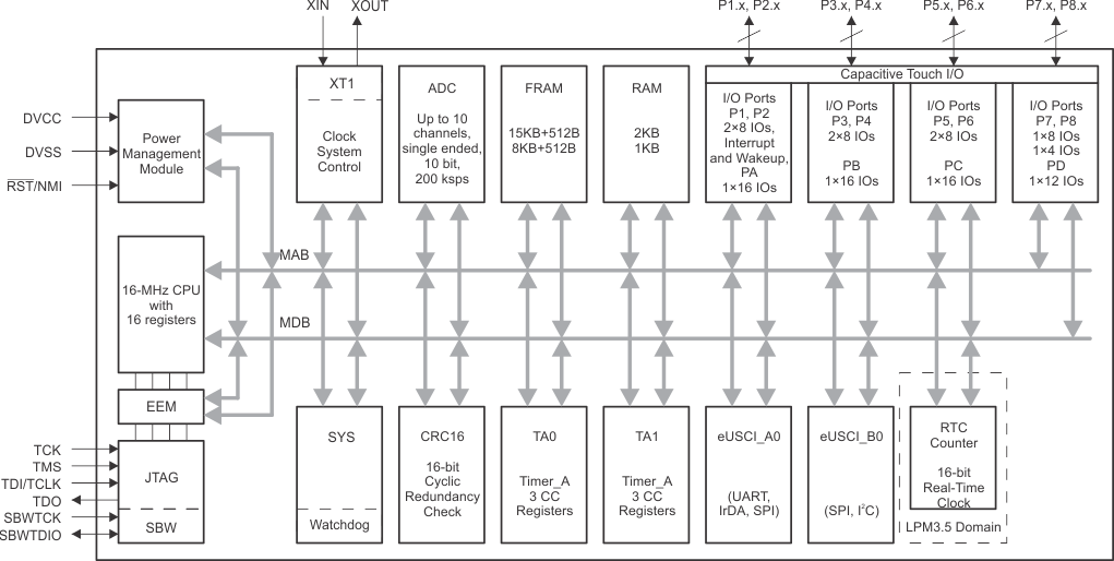
1.4 Functional Block Diagram
Figure 1-1 shows the functional block diagram.
 Figure 1-1 Functional Block Diagram
 - The device has one main power pair of DVCC and DVSS that supplies both digital and analog modules. Recommended bypass and decoupling capacitors are 4.7 µF to 10 µF and 0.1 µF, respectively, with ±5% accuracy.
- P1 and P2 feature the pin-interrupt function and can wake the MCU from LPM3.5.
- Each Timer_A3 has three CC registers, but only the CCR1 and CCR2 are externally connected. CCR0 registers can only be used for internal period timing and interrupt generation.
- In LPM3.5, the RTC counter can be functional while the remaining peripherals are off.
- Not all I/Os are bonded in TSSOP-56 and TSSOP-48 packages (refer to Table 4-1). All I/Os can be configured as Capacitive Touch I/Os.