SLASEK0A December 2017 – March 2018 MSP430FR5969-SP
PRODUCTION DATA.
- 1Device Overview
- 2Revision History
- 3Terminal Configuration and Functions
-
4Specifications
- 4.1 Absolute Maximum Ratings
- 4.2 ESD Ratings
- 4.3 Recommended Operating Conditions
- 4.4 Active Mode Supply Current Into VCC Excluding External Current
- 4.5 Typical Characteristics – Active Mode Supply Currents
- 4.6 Low-Power Mode (LPM0, LPM1) Supply Currents Into VCC Excluding External Current
- 4.7 Low-Power Mode (LPM2, LPM3, LPM4) Supply Currents (Into VCC) Excluding External Current
- 4.8 Low-Power Mode (LPM3.5, LPM4.5) Supply Currents (Into VCC) Excluding External Current
- 4.9 Typical Characteristics, Current Consumption per Module
- 4.10 Thermal Resistance Characteristics
- 4.11
Timing and Switching Characteristics
- 4.11.1 Power Supply Sequencing
- 4.11.2 Reset Timing
- 4.11.3 Clock Specifications
- 4.11.4 Wake-up Characteristics
- 4.11.5 Digital I/Os
- 4.11.6 Timer_A and Timer_B
- 4.11.7 eUSCI
- 4.11.8
ADC
- Table 4-22 12-Bit ADC, Power Supply and Input Range Conditions
- Table 4-23 12-Bit ADC, Timing Parameters
- Table 4-24 12-Bit ADC, Linearity Parameters With External Reference
- Table 4-25 12-Bit ADC, Dynamic Performance for Differential Inputs With External Reference
- Table 4-26 12-Bit ADC, Dynamic Performance for Differential Inputs With Internal Reference
- Table 4-27 12-Bit ADC, Dynamic Performance for Single-Ended Inputs With External Reference
- Table 4-28 12-Bit ADC, Dynamic Performance for Single-Ended Inputs With Internal Reference
- Table 4-29 12-Bit ADC, Dynamic Performance With 32.768-kHz Clock
- Table 4-30 12-Bit ADC, Temperature Sensor and Built-In V1/2
- Table 4-31 12-Bit ADC, External Reference
- 4.11.9 Reference
- 4.11.10 Comparator
- 4.11.11 FRAM
- 4.12 Emulation and Debug
-
5Detailed Description
- 5.1 Overview
- 5.2 CPU
- 5.3 Operating Modes
- 5.4 Interrupt Vector Table and Signatures
- 5.5 Memory Organization
- 5.6 Bootloader (BSL)
- 5.7 JTAG Operation
- 5.8 FRAM
- 5.9 Memory Protection Unit Including IP Encapsulation
- 5.10
Peripherals
- 5.10.1 Digital I/O
- 5.10.2 Oscillator and Clock System (CS)
- 5.10.3 Power-Management Module (PMM)
- 5.10.4 Hardware Multiplier (MPY)
- 5.10.5 Real-Time Clock (RTC_B) (Only MSP430FR596x and MSP430FR594x)
- 5.10.6 Watchdog Timer (WDT_A)
- 5.10.7 System Module (SYS)
- 5.10.8 DMA Controller
- 5.10.9 Enhanced Universal Serial Communication Interface (eUSCI)
- 5.10.10 TA0, TA1
- 5.10.11 TA2, TA3
- 5.10.12 TB0
- 5.10.13 ADC12_B
- 5.10.14 Comparator_E
- 5.10.15 CRC16
- 5.10.16 AES256 Accelerator
- 5.10.17 True Random Seed
- 5.10.18 Shared Reference (REF)
- 5.10.19 Embedded Emulation
- 5.10.20 Peripheral File Map
- 5.11
Input and Output Diagrams
- 5.11.1 Port P1 (P1.0 to P1.2) Input/Output With Schmitt Trigger
- 5.11.2 Port P1 (P1.3 to P1.5) Input/Output With Schmitt Trigger
- 5.11.3 Port P1 (P1.6 and P1.7) Input/Output With Schmitt Trigger
- 5.11.4 Port P2 (P2.0 to P2.2) Input/Output With Schmitt Trigger
- 5.11.5 Port P2 (P2.3 and P2.4) Input/Output With Schmitt Trigger
- 5.11.6 Port P2 (P2.5 and P2.6) Input/Output With Schmitt Trigger
- 5.11.7 Port P2 (P2.7) Input/Output With Schmitt Trigger
- 5.11.8 Port P3 (P3.0 to P3.3) Input/Output With Schmitt Trigger
- 5.11.9 Port P3 (P3.4 to P3.7) Input/Output With Schmitt Trigger
- 5.11.10 Port P4 (P4.0 to P4.3) Input/Output With Schmitt Trigger
- 5.11.11 Port P4 (P4.4 to P4.7) Input/Output With Schmitt Trigger
- 5.11.12 Port PJ, PJ.4 and PJ.5 Input/Output With Schmitt Trigger
- 5.11.13 Port PJ (PJ.6 and PJ.7) Input/Output With Schmitt Trigger
- 5.11.14 Port PJ (PJ.0 to PJ.3) JTAG Pins TDO, TMS, TCK, TDI/TCLK, Input/Output With Schmitt Trigger
- 5.12 Device Descriptor (TLV)
- 5.13 Identification
- 6Applications, Implementation, and Layout
- 7Device and Documentation Support
- 8Mechanical, Packaging, and Orderable Information
Package Options
Mechanical Data (Package|Pins)
Thermal pad, mechanical data (Package|Pins)
Orderable Information
Table 4-30 12-Bit ADC, Temperature Sensor and Built-In V1/2
over recommended ranges of supply voltage and operating temperature (unless otherwise noted)| PARAMETER | TEST CONDITIONS | MIN | TYP | MAX | UNIT | |
|---|---|---|---|---|---|---|
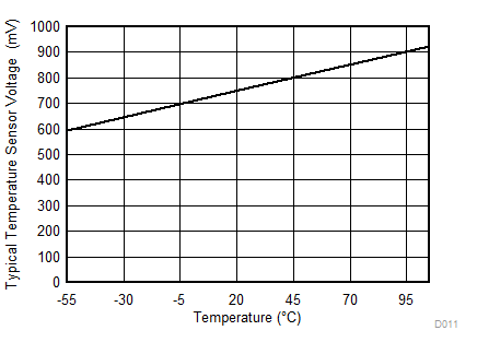
| VSENSOR | See (1)(2) (also see Figure 4-16) | ADC12ON = 1, ADC12TCMAP = 1,
TA = 0°C |
700 | mV | ||
| TCSENSOR | See (2) | ADC12ON = 1, ADC12TCMAP = 1 | 2.5 | mV/°C | ||
| tSENSOR(sample) | Sample time required if ADCTCMAP = 1 and channel (MAX – 1) is selected(3) | ADC12ON = 1, ADC12TCMAP = 1,
Error of conversion result ≤ 1 LSB |
30 | µs | ||
| V1/2 | AVCC voltage divider for ADC12BATMAP = 1 on MAX input channel | ADC12ON = 1, ADC12BATMAP = 1 | 47.5% | 50% | 52.5% | |
| IV 1/2 | Current for battery monitor during sample time | ADC12ON = 1, ADC12BATMAP = 1 | 38 | 63 | µA | |
| tV 1/2 (sample) | Sample time required if ADC12BATMAP = 1 and channel MAX is selected(4) | ADC12ON = 1, ADC12BATMAP = 1 | 1.7 | µs | ||
(1) The temperature sensor offset can be as much as ±30°C. TI recommends a single-point calibration to minimize the offset error of the built-in temperature sensor.
(2) The device descriptor structure contains calibration values for 30°C ±3°C and 105°C ±3°C for each available reference voltage level. The sensor voltage can be computed as VSENSE = TCSENSOR × (Temperature, °C) + VSENSOR, where TCSENSOR and VSENSOR can be computed from the calibration values for higher accuracy.
(3) The typical equivalent impedance of the sensor is 250 kΩ. The sample time required includes the sensor-on time tSENSOR(on).
(4) The on-time tV1/2(on) is included in the sampling time tV1/2(sample); no additional on time is needed.
 Figure 4-16 Typical Temperature Sensor Voltage
Table 4-31 lists the external reference requirements for the ADC.