SLASEX5C October 2022 – January 2024 MSPM0L1105 , MSPM0L1106
PRODUCTION DATA
- 1
- 1 Features
- 2 Applications
- 3 Description
- 4 Functional Block Diagram
- 5 Device Comparison
- 6 Pin Configuration and Functions
-
7 Specifications
- 7.1 Absolute Maximum Ratings
- 7.2 ESD Ratings
- 7.3 Recommended Operating Conditions
- 7.4 Thermal Information
- 7.5 Supply Current Characteristics
- 7.6 Power Supply Sequencing
- 7.7 Flash Memory Characteristics
- 7.8 Timing Characteristics
- 7.9 Clock Specifications
- 7.10 Digital IO
- 7.11 Analog Mux VBOOST
- 7.12 ADC
- 7.13 Temperature Sensor
- 7.14 VREF
- 7.15 GPAMP
- 7.16 I2C
- 7.17 SPI
- 7.18 UART
- 7.19 TIMx
- 7.20 Emulation and Debug
-
8 Detailed Description
- 8.1 CPU
- 8.2 Operating Modes
- 8.3 Power Management Unit (PMU)
- 8.4 Clock Module (CKM)
- 8.5 DMA
- 8.6 Events
- 8.7 Memory
- 8.8 Flash Memory
- 8.9 SRAM
- 8.10 GPIO
- 8.11 IOMUX
- 8.12 ADC
- 8.13 Temperature Sensor
- 8.14 VREF
- 8.15 GPAMP
- 8.16 CRC
- 8.17 UART
- 8.18 SPI
- 8.19 I2C
- 8.20 WWDT
- 8.21 Timers (TIMx)
- 8.22 Device Analog Connections
- 8.23 Input/Output Diagrams
- 8.24 Bootstrap Loader (BSL)
- 8.25 Serial Wire Debug Interface
- 8.26 Device Factory Constants
- 8.27 Identification
- 9 Applications, Implementation, and Layout
- 10Device and Documentation Support
- 11Revision History
- 12Mechanical, Packaging, and Orderable Information
Package Options
Refer to the PDF data sheet for device specific package drawings
Mechanical Data (Package|Pins)
- DGS|28
- DYY|16
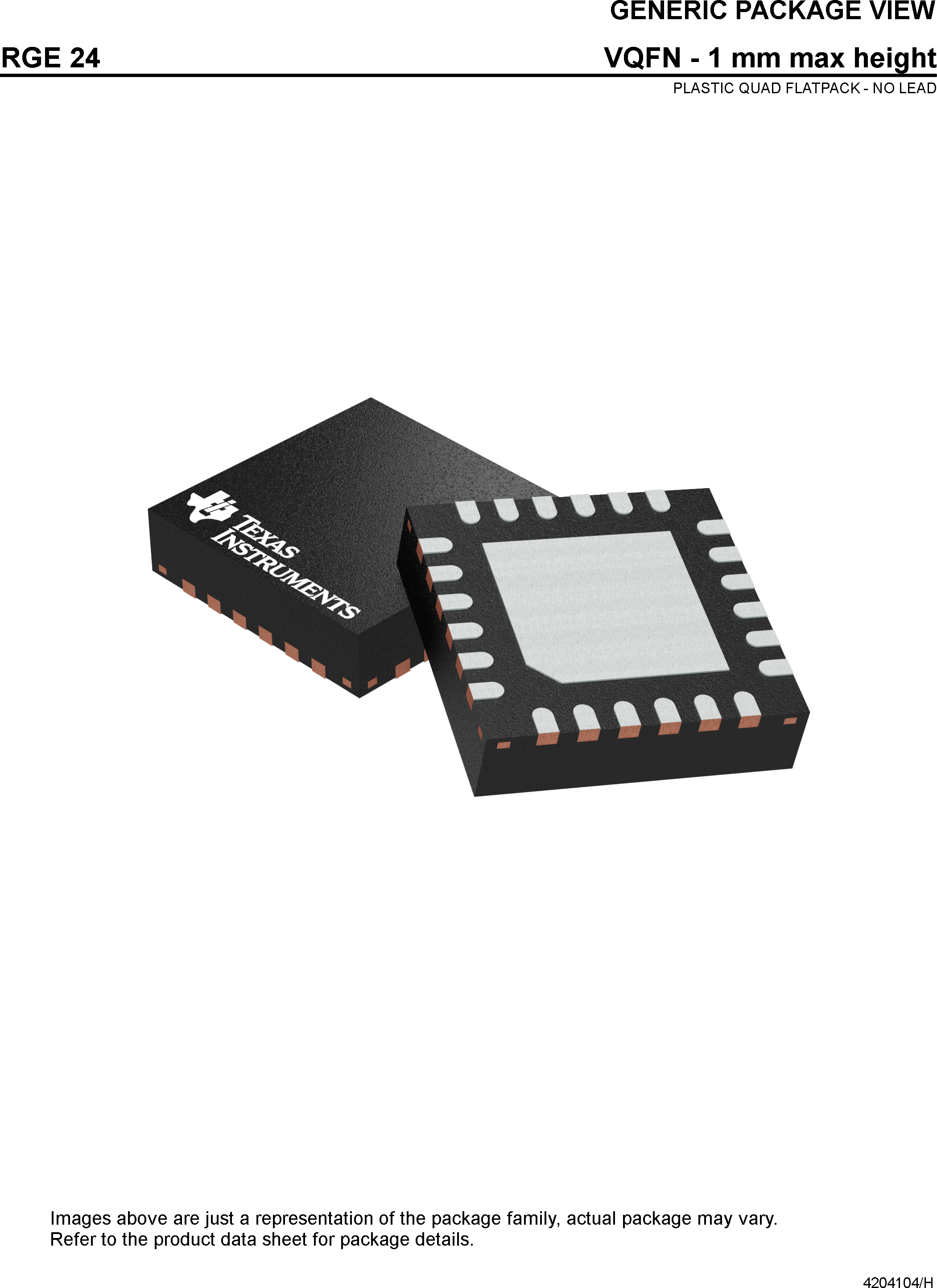
- RGE|24
- RHB|32
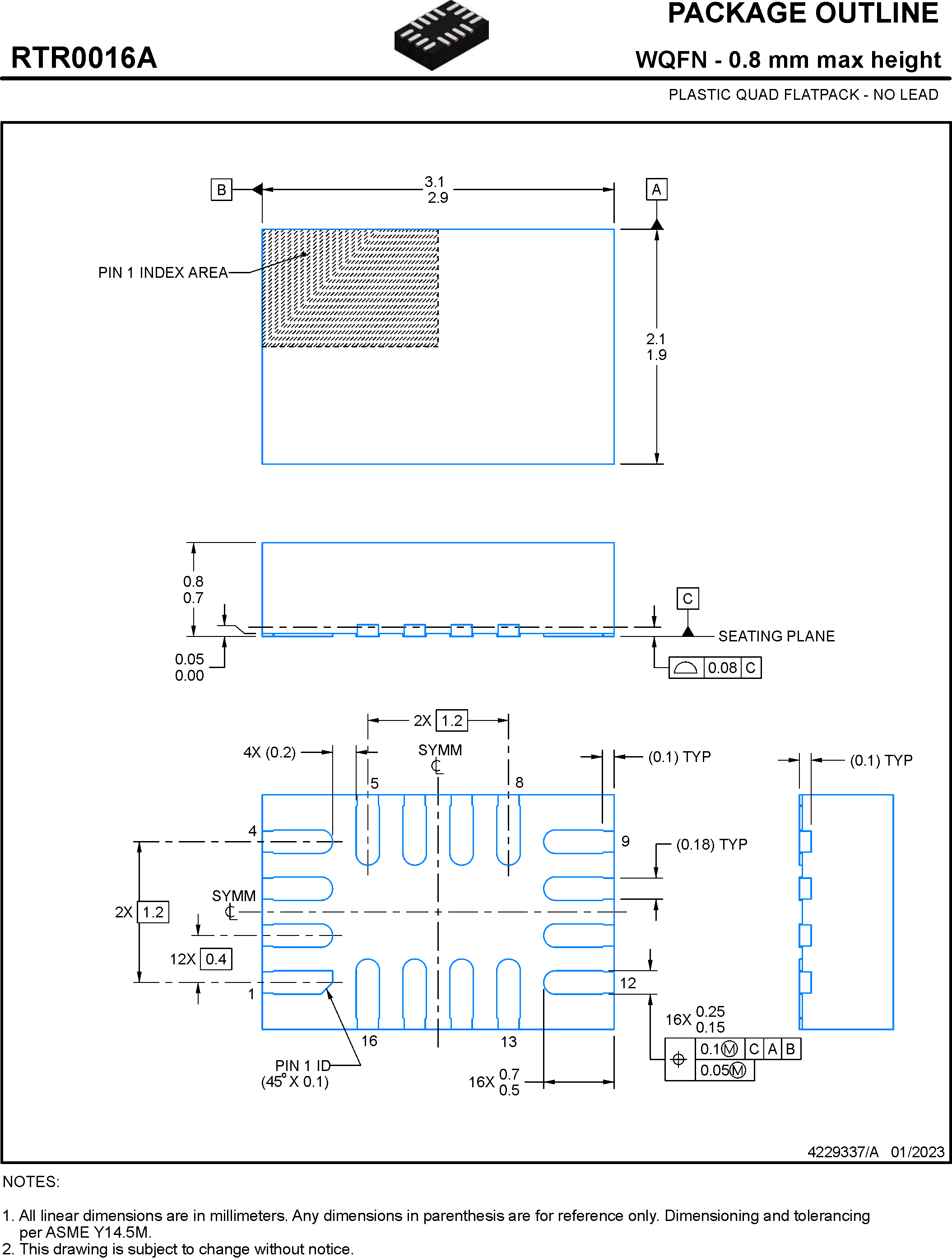
- RTR|16
- DGS|20
Thermal pad, mechanical data (Package|Pins)
Orderable Information
12 Mechanical, Packaging, and Orderable Information
The following pages include mechanical, packaging, and orderable information. This information is the most current data available for the designated devices. This data is subject to change without notice and revision of this document. For browser-based versions of this data sheet, refer to the left-hand navigation.