SBOS705D January 2016 – Feburary 2019 MUX36D04 , MUX36S08
PRODUCTION DATA.
- 1 Features
- 2 Applications
- 3 Description
- 4 Revision History
- 5 Device Comparison Table
- 6 Pin Configuration and Functions
- 7 Specifications
-
8 Parameter Measurement Information
- 8.1 Truth Tables
- 8.2 On-Resistance
- 8.3 Off-Leakage Current
- 8.4 On-Leakage Current
- 8.5 Differential On-Leakage Current
- 8.6 Transition Time
- 8.7 Break-Before-Make Delay
- 8.8 Turn-On and Turn-Off Time
- 8.9 Charge Injection
- 8.10 Off Isolation
- 8.11 Channel-to-Channel Crosstalk
- 8.12 Bandwidth
- 8.13 THD + Noise
- 9 Detailed Description
- 10Application and Implementation
- 11Power Supply Recommendations
- 12Layout
- 13Device and Documentation Support
- 14Mechanical, Packaging, and Orderable Information
Package Options
Mechanical Data (Package|Pins)
Thermal pad, mechanical data (Package|Pins)
- RUM|16
Orderable Information
8.11 Channel-to-Channel Crosstalk
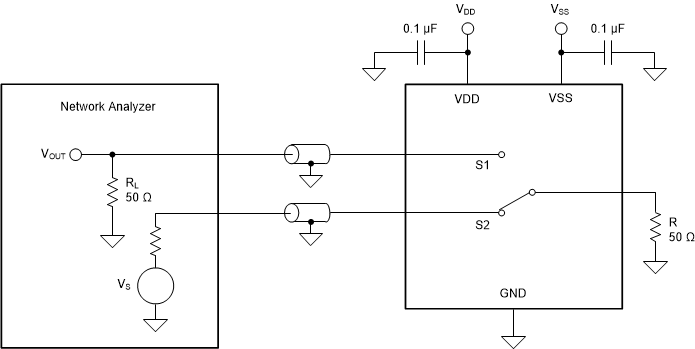
Channel-to-channel crosstalk is defined as the voltage at the source pin (Sx, SxA, or SxB) of an off-channel, when a 1-VRMS signal is applied at the source pin of an on-channel. Figure 35 shows the setup used to measure, and Equation 3 is the equation used to compute, channel-to-channel crosstalk.
 Figure 35. Channel-to-Channel Crosstalk Measurement Setup
 Equation 3. 
