SLFS022I September 1973 – September 2014 NA555 , NE555 , SA555 , SE555
PRODUCTION DATA.
- 1 Features
- 2 Applications
- 3 Description
- 4 Simplified Schematic
- 5 Revision History
- 6 Pin Configuration and Functions
- 7 Specifications
- 8 Detailed Description
- 9 Applications and Implementation
- 10Power Supply Recommendations
- 11Device and Documentation Support
- 12Mechanical, Packaging, and Orderable Information
Package Options
Mechanical Data (Package|Pins)
Thermal pad, mechanical data (Package|Pins)
Orderable Information
7 Specifications
7.1 Absolute Maximum Ratings(1)
over operating free-air temperature range (unless otherwise noted)| MIN | MAX | UNIT | |||
|---|---|---|---|---|---|
| VCC | Supply voltage(2) | 18 | V | ||
| VI | Input voltage | CONT, RESET, THRES, TRIG | VCC | V | |
| IO | Output current | ±225 | mA | ||
| θJA | Package thermal impedance(3)(4) | D package | 97 | °C/W | |
| P package | 85 | ||||
| PS package | 95 | ||||
| PW package | 149 | ||||
| θJC | Package thermal impedance(5)(6) | FK package | 5.61 | °C/W | |
| JG package | 14.5 | ||||
| TJ | Operating virtual junction temperature | 150 | °C | ||
| Case temperature for 60 s | FK package | 260 | °C | ||
| Lead temperature 1,6 mm (1/16 in) from case for 60 s | JG package | 300 | °C | ||
(1) Stresses beyond those listed under Absolute Maximum Ratings may cause permanent damage to the device. These are stress ratings only, and functional operation of the device at these or any other conditions beyond those indicated under Recommended Operating Conditions is not implied. Exposure to absolute-maximum-rated conditions for extended periods may affect device reliability.
(2) All voltage values are with respect to GND.
(3) Maximum power dissipation is a function of TJ(max), θJA, and TA. The maximum allowable power dissipation at any allowable ambient temperature is PD = (TJ(max) - TA) / θJA. Operating at the absolute maximum TJ of 150°C can affect reliability.
(4) The package thermal impedance is calculated in accordance with JESD 51-7.
(5) Maximum power dissipation is a function of TJ(max), θJC, and TC. The maximum allowable power dissipation at any allowable case temperature is PD = (TJ(max) - TC) / θJC. Operating at the absolute maximum TJ of 150°C can affect reliability.
(6) The package thermal impedance is calculated in accordance with MIL-STD-883.
7.3 Recommended Operating Conditions
over operating free-air temperature range (unless otherwise noted)| MIN | MAX | UNIT | |||
|---|---|---|---|---|---|
| VCC | Supply voltage | NA555, NE555, SA555 | 4.5 | 16 | V |
| SE555 | 4.5 | 18 | |||
| VI | Input voltage | CONT, RESET, THRES, and TRIG | VCC | V | |
| IO | Output current | ±200 | mA | ||
| TA | Operating free-air temperature | NA555 | –40 | 105 | °C |
| NE555 | 0 | 70 | |||
| SA555 | –40 | 85 | |||
| SE555 | –55 | 125 | |||
7.4 Electrical Characteristics
VCC = 5 V to 15 V, TA = 25°C (unless otherwise noted)| PARAMETER | TEST CONDITIONS | SE555 | NA555 NE555 SA555 |
UNIT | |||||
|---|---|---|---|---|---|---|---|---|---|
| MIN | TYP | MAX | MIN | TYP | MAX | ||||
| THRES voltage level | VCC = 15 V | 9.4 | 10 | 10.6 | 8.8 | 10 | 11.2 | V | |
| VCC = 5 V | 2.7 | 3.3 | 4 | 2.4 | 3.3 | 4.2 | |||
| THRES current(1) | 30 | 250 | 30 | 250 | nA | ||||
| TRIG voltage level | VCC = 15 V | 4.8 | 5 | 5.2 | 4.5 | 5 | 5.6 | V | |
| TA = –55°C to 125°C | 3 | 6 | |||||||
| VCC = 5 V | 1.45 | 1.67 | 1.9 | 1.1 | 1.67 | 2.2 | |||
| TA = –55°C to 125°C | 1.9 | ||||||||
| TRIG current | TRIG at 0 V | 0.5 | 0.9 | 0.5 | 2 | μA | |||
| RESET voltage level | 0.3 | 0.7 | 1 | 0.3 | 0.7 | 1 | V | ||
| TA = –55°C to 125°C | 1.1 | ||||||||
| RESET current | RESET at VCC | 0.1 | 0.4 | 0.1 | 0.4 | mA | |||
| RESET at 0 V | –0.4 | –1 | –0.4 | –1.5 | |||||
| DISCH switch off-state current | 20 | 100 | 20 | 100 | nA | ||||
| DISCH switch on-state voltage | VCC = 5 V, IO = 8 mA | 0.15 | 0.4 | V | |||||
| CONT voltage (open circuit) | VCC = 15 V | 9.6 | 10 | 10.4 | 9 | 10 | 11 | V | |
| TA = –55°C to 125°C | 9.6 | 10.4 | |||||||
| VCC = 5 V | 2.9 | 3.3 | 3.8 | 2.6 | 3.3 | 4 | |||
| TA = –55°C to 125°C | 2.9 | 3.8 | |||||||
| Low-level output voltage | VCC = 15 V, IOL = 10 mA | 0.1 | 0.15 | 0.1 | 0.25 | V | |||
| TA = –55°C to 125°C | 0.2 | ||||||||
| VCC = 15 V, IOL = 50 mA | 0.4 | 0.5 | 0.4 | 0.75 | |||||
| TA = –55°C to 125°C | 1 | ||||||||
| VCC = 15 V, IOL = 100 mA | 2 | 2.2 | 2 | 2.5 | |||||
| TA = –55°C to 125°C | 2.7 | ||||||||
| VCC = 15 V, IOL = 200 mA | 2.5 | 2.5 | |||||||
| VCC = 5 V, IOL = 3.5 mA | TA = –55°C to 125°C | 0.35 | |||||||
| VCC = 5 V, IOL = 5 mA | 0.1 | 0.2 | 0.1 | 0.35 | |||||
| TA = –55°C to 125°C | 0.8 | ||||||||
| VCC = 5 V, IOL = 8 mA | 0.15 | 0.25 | 0.15 | 0.4 | |||||
| High-level output voltage | VCC = 15 V, IOH = –100 mA | 13 | 13.3 | 12.75 | 13.3 | V | |||
| TA = –55°C to 125°C | 12 | ||||||||
| VCC = 15 V, IOH = –200 mA | 12.5 | 12.5 | |||||||
| VCC = 5 V, IOH = –100 mA | 3 | 3.3 | 2.75 | 3.3 | |||||
| TA = –55°C to 125°C | 2 | ||||||||
| Supply current | Output low, No load | VCC = 15 V | 10 | 12 | 10 | 15 | mA | ||
| VCC = 5 V | 3 | 5 | 3 | 6 | |||||
| Output high, No load | VCC = 15 V | 9 | 10 | 9 | 13 | ||||
| VCC = 5 V | 2 | 4 | 2 | 5 | |||||
(1) This parameter influences the maximum value of the timing resistors RA and RB in the circuit of Figure 12. For example,
when VCC = 5 V, the maximum value is R = RA + RB ≉ 3.4 MΩ, and for VCC = 15 V, the maximum value is 10 MΩ.
when VCC = 5 V, the maximum value is R = RA + RB ≉ 3.4 MΩ, and for VCC = 15 V, the maximum value is 10 MΩ.
7.5 Operating Characteristics
VCC = 5 V to 15 V, TA = 25°C (unless otherwise noted)| PARAMETER | TEST CONDITIONS(2) |
SE555 | NA555 NE555 SA555 |
UNIT | |||||
|---|---|---|---|---|---|---|---|---|---|
| MIN | TYP | MAX | MIN | TYP | MAX | ||||
| Initial error of timing interval(3) | Each timer, monostable(4) | TA = 25°C | 0.5 | 1.5(1) | 1 | 3 | % | ||
| Each timer, astable(5) | 1.5 | 2.25 | |||||||
| Temperature coefficient of timing interval | Each timer, monostable(4) | TA = MIN to MAX | 30 | 100(1) | 50 | ppm/ °C |
|||
| Each timer, astable(5) | 90 | 150 | |||||||
| Supply-voltage sensitivity of timing interval | Each timer, monostable(4) | TA = 25°C | 0.05 | 0.2(1) | 0.1 | 0.5 | %/V | ||
| Each timer, astable(5) | 0.15 | 0.3 | |||||||
| Output-pulse rise time | CL = 15 pF, TA = 25°C |
100 | 200(1) | 100 | 300 | ns | |||
| Output-pulse fall time | CL = 15 pF, TA = 25°C |
100 | 200(1) | 100 | 300 | ns | |||
(1) On products compliant to MIL-PRF-38535, this parameter is not production tested.
(2) For conditions shown as MIN or MAX, use the appropriate value specified under recommended operating conditions.
(3) Timing interval error is defined as the difference between the measured value and the average value of a random sample from each process run.
(4) Values specified are for a device in a monostable circuit similar to Figure 9, with the following component values: RA = 2 kΩ to 100 kΩ, C = 0.1 μF.
(5) Values specified are for a device in an astable circuit similar to Figure 12, with the following component values: RA = 1 kΩ to 100 kΩ, C = 0.1 μF.
7.6 Typical Characteristics
Data for temperatures below –40°C and above 105°C are applicable for SE555 circuits only.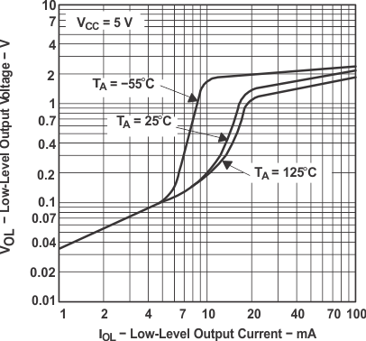 Figure 1. Low-Level Output Voltage
 vs Low-Level Output Current
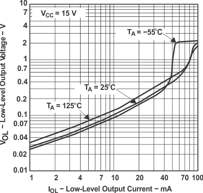 Figure 3. Low-Level Output Voltage
 vs Low-Level Output Current
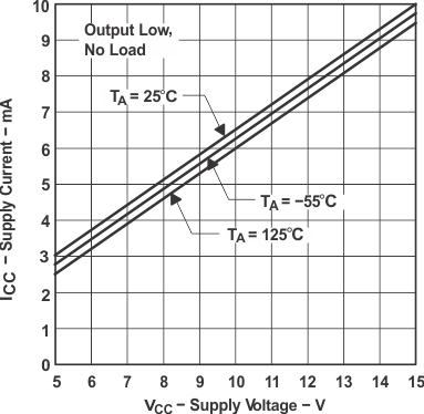 Figure 5. Supply Current
 vs Supply Voltage
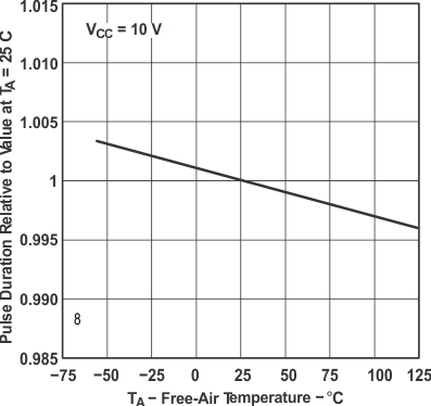 Figure 7. Normalized Output Pulse Duration
 (Monostable Operation)
vs
Free-Air Temperature
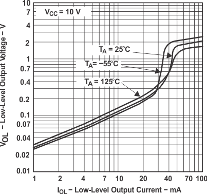 Figure 2. Low-Level Output Voltage
 vs Low-Level Output Current
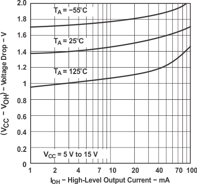 Figure 4. Drop Between Supply Voltage and Output
 vs High-Level Output Current
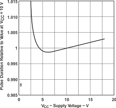 Figure 6. Normalized Output Pulse Duration
 (Monostable Operation)
vs Supply Voltage
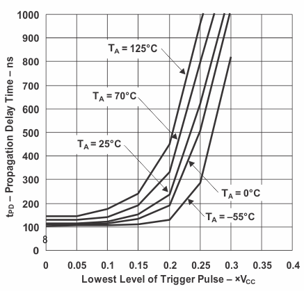 Figure 8. Propagation Delay Time
 vs
Lowest Voltage Level of Trigger Pulse