SLLSEO4A June 2015 – July 2015 ONET1130EP
PRODUCTION DATA.
- 1 Features
- 2 Applications
- 3 Description
- 4 Revision History
- 5 Description (continued)
- 6 Pin Configuration and Function
- 7 Specifications
-
8 Detailed Description
- 8.1 Overview
- 8.2 Functional Block Diagram
- 8.3 Feature Description
- 8.4 Device Functional Modes
- 8.5 Programming
- 8.6
Register Mapping
- 8.6.1 R/W Control Registers
- 8.6.2
RX Registers
- 8.6.2.1 RX Register 4 (offset = 0000 0000) [reset = 0h]
- 8.6.2.2 RX Register 5 (offset = 0000 0000) [reset = 0h]
- 8.6.2.3 RX Register 6 (offset = 0000 0000) [reset = 0h]
- 8.6.2.4 RX Register 7 (offset = 0000 0000) [reset = 0h]
- 8.6.2.5 RX Register 8 (offset = 0000 0000) [reset = 0h]
- 8.6.2.6 RX Register 9 (offset = 0000 0000) [reset = 0h]
- 8.6.3
TX Registers
- 8.6.3.1 TX Register 10 (offset = 0000 0000) [reset = 0h]
- 8.6.3.2 TX Register 11 (offset = 0000 0000) [reset = 0h]
- 8.6.3.3 TX Register 12 (offset = 0000 0000) [reset = 0h]
- 8.6.3.4 TX Register 13 (offset = 0h) [reset = 0]
- 8.6.3.5 TX Register 14 (offset = 0000 0000) [reset = 0h]
- 8.6.3.6 TX Register 15 (offset = 0000 0000) [reset = 0h]
- 8.6.3.7 TX Register 16 (offset = 0000 0000) [reset = 0h]
- 8.6.3.8 TX Register 17 (offset = 0000 0000) [reset = 0h]
- 8.6.3.9 TX Register 18 (offset = 0000 0000) [reset = 0h]
- 8.6.4 Reserved Registers
- 8.6.5 Read Only Registers
- 8.6.6 Adjustment Registers
- 9 Application Information and Implementations
- 10Power Supply Recommendations
- 11Layout
- 12Device and Documentation Support
- 13Mechanical, Packaging, and Orderable Information
Package Options
Mechanical Data (Package|Pins)
- RSM|32
Thermal pad, mechanical data (Package|Pins)
- RSM|32
Orderable Information
7 Specifications
7.1 Absolute Maximum Ratings (1)(2)
over operating free-air temperature range (unless otherwise noted)| MIN | MAX | UNIT | ||
|---|---|---|---|---|
| Supply voltage | at VCC_TX, VCC_RX, VDD | –0.5 | 3 | V |
| Voltage | at 3.3-V tolerant pinsSDA, SCK, RX_LOS, RX_DIS, TX_FLT, TX_DIS | –0.5 | 3.6 | V |
| at all other pins MONB, TXIN+, TXIN–, PD, MONP, BIAS, TXOUT–, TXOUT+, AMP, RXIN+, RXIN–, COMP, RX_LF, RXOUT–, RXOUT+, | –0.5 | 3 | V | |
| Maximum current at transmitter input pins | TXIN+, TXIN– | 10 | mA | |
| Maximum current at transmitter output pins | TXOUT+, TXOUT– | 125 | mA | |
| Maximum current at receiver input pins | RXIN+, RXIN– | 10 | mA | |
| Maximum current at receiver output pins | RXOUT+, RXOUT– | 30 | mA | |
| Maximum junction temperature, TJ | 125 | °C | ||
| Storage temperature, Tstg | –65 | 150 | °C | |
(1) Stresses beyond those listed under “absolute maximum ratings” may cause permanent damage to the device. These are stress ratings only and functional operation of the device at these or any other conditions beyond those indicated under “recommended operating conditions” is not implied. Exposure to absolute–maximum–rated conditions for extended periods may affect device reliability.
(2) All voltage values are with respect to network ground terminal.
7.2 ESD Ratings
| VALUE | UNIT | |||
|---|---|---|---|---|
| V(ESD) | Electrostatic discharge | Human-body model (HBM), per ANSI/ESDA/JEDEC JS-001(1) | ±2000 | V |
| Charged-device model (CDM), per JEDEC specification JESD22-C101(2) | ±750 | |||
(1) JEDEC document JEP155 states that 500-V HBM allows safe manufacturing with a standard ESD control process.
(2) JEDEC document JEP157 states that 250-V CDM allows safe manufacturing with a standard ESD control process.
7.3 Recommended Operating Conditions
over operating free-air temperature range (unless otherwise noted)| MIN | TYP | MAX | UNIT | |||
|---|---|---|---|---|---|---|
| VCC | Supply Voltage | 2.37 | 2.5 | 2.63 | V | |
| VIH | Digital input high voltage | TX_DIS, RX_DIS, SCK, SDA, 3.3-V tolerant IOs | 2 | V | ||
| VIL | Digital input low voltage | 0.8 | V | |||
| Photodiode current range | Control bit TXPDRNG = 1x, step size = 3 µA | 3080 | µA | |||
| Control bit TXPDRNG = 01, step size = 1.5 µA | 1540 | |||||
| Control bit TXPDRNG = 00, step size = 0.75 µA | 770 | |||||
| Serial Data rate | 11.7 | Gbps | ||||
| VAMP | Amplitude control input voltage range | 0 | 2 | V | ||
| tR-IN | Input rise time | 20%–80% | 30 | 45 | ps | |
| tF-IN | Input fall time | 20%–80% | 30 | 45 | ps | |
| TC | Temperature at thermal pad | –40 | 100 | °C | ||
7.4 Thermal Information
| THERMAL METRIC(1) | RSM (VQFN) | UNIT | |
|---|---|---|---|
| 32 PINS | |||
| RθJA | Junction-to-ambient thermal resistance | 37.2 | °C/W |
| RθJCtop | Junction-to-case (top) thermal resistance | 30.1 | °C/W |
| RθJB | Junction-to-board thermal resistance | 7.8 | °C/W |
| ψJT | Junction-to-top characterization parameter | 0.4 | °C/W |
| ψJB | Junction-to-board characterization parameter | 7.6 | °C/W |
| RθJCbot | Junction-to-case (bottom) thermal resistance | 2.4 | °C/W |
(1) For more information about traditional and new thermal metrics, see the Semiconductor and IC Package Thermal Metrics application report, SPRA953.
7.5 DC Electrical Characteristics
Over recommended operating conditions, open loop operation, VOUT = 2 VPP single-ended, I(BIAS) = 80 mA, unless otherwise noted. Typical operating condition is at VCC = 2.5 V and TA = 25°C| PARAMETER | TEST CONDITIONS | MIN | TYP | MAX | UNIT | |
|---|---|---|---|---|---|---|
| VCC | Supply voltage | 2.37 | 2.5 | 2.63 | V | |
| IVCC | Supply current in single-ended TX mode | TXMODE = 1, TX VOUT = 2 VPP single-ended, I(BIAS) = 0 mA; 600 mVPP differential RX output | 161 | 185 | mA | |
| Power dissipation in single-ended TX mode | 403 | 487 | mW | |||
| Supply current in differential TX mode | TXMODE = 0, TX VOUT = 1.8 VPP single-ended, I(BIAS) = 0 mA; 600 mVPP differential RX output | 206 | 242 | mA | ||
| Power dissipation in differential TX mode | 515 | 636 | mW | |||
| R(TXIN) | Transmitter data input resistance | Differential between TXIN+ / TXIN– | 100 | Ω | ||
| Transmitter data input termination mismatch | 5% | |||||
| R(RXIN) | Receiver data input resistance | Differential between RXIN+ / RXIN– | 100 | Ω | ||
| R(OUT) | Transmitter output resistance | Single-ended at TXOUT+ or TXOUT– | 60 | Ω | ||
| R(RXOUT) | Receiver data output resistance | Differential between RXOUT+ or RXOUT– | 90 | Ω | ||
| Receiver data output termination mismatch | 5% | |||||
| Digital input current | TX_DIS, RX_DIS pull up to VCC | –20 | 20 | µA | ||
| VOH | Digital output high voltage | TX_FLT, RX_LOS, pull-up to VCC, ISOURCE = 37.5 μA |
2.1 | V | ||
| VOL | Digital output low voltage | TX_FLT, RX_LOS, pull-up to VCC, ISINK = 350 μA |
0.4 | V | ||
| I(BIAS-MIN) | Minimum bias current | See (1) | 5 | mA | ||
| I(BIAS-MAX) | Maximum bias current | Source. BIASPOL = 0, DAC set to maximum, open and closed loop | 145 | 150 | mA | |
| Sink. BIASPOL = 1, DAC set to maximum, open and closed loop | 95 | 100 | ||||
| I(BIAS-DIS) | Bias current during disable | 100 | µA | |||
| Average power stability | APC loop enabled | ±0.5 | dB | |||
| Bias pin compliance voltage | Source. TXBIASPOL = 0 | VCC-0.45 | V | |||
| Sink. TXBIASPOL = 1 | 0.45 | |||||
| Temperature sensor accuracy | With 1-point external mid-scale calibration | ±3 | °C | |||
| V(PD) | Photodiode reverse bias voltage | APC active, I(PD) = 1500 μA | 1.3 | 2.3 | V | |
| Photodiode fault current level | Percent of target I(PD)(2) | 150% | ||||
| Photodiode current monitor ratio | I(MONP) / I(PD) with control bit PDRNG = 1X | 10% | 12.5% | 15% | ||
| I(MONP) / I(PD) with control bit PDRNG = 01 | 20% | 25% | 30% | |||
| I(MONP) / I(PD) with control bit TXPDRNG = 00 | 40% | 50% | 60% | |||
| Monitor diode DMI accuracy | With external mid-scale calibration | ±10% | ||||
| Bias current monitor ratio | I(MONB) / I(BIAS) (nominal 1/100 = 1%), V(MONB) < 1.5V | 0.9% | 1% | 1.1% | ||
| Bias current DMI accuracy | I(BIAS) ≥ 20 mA | –15% | 15% | |||
| Power supply monitor accuracy | With external mid-scale calibration | –2% | 2% | |||
| V(CC-RST) | VCC reset threshold voltage | VCC voltage level which triggers power-on reset | 1.8 | 2.1 | V | |
| V(CC-RSTHYS) | VCC reset threshold voltage hysteresis | 100 | mV | |||
| V(MONB-FLT) | Fault voltage at MONB | TXFLTEN = 1, TXDMONB = 0, Fault occurs if voltage at MONB exceeds this value | 1.15 | 1.2 | 1.25 | V |
| V(MONP-FLT) | Fault voltage at MONP | TXFLTEN = 1, TXMONPFLT = 1, TXDMONP = 0, Fault occurs if voltage at MONP exceeds this value | 1.15 | 1.2 | 1.25 | V |
(1) The bias current can be set below the specified minimum according to the corresponding register setting; however, in closed loop operation settings below the specified value may trigger a fault.
(2) Assured by design over process, supply and temperature variation
7.6 Transmitter AC Electrical Characteristics
Over recommended operating conditions, open loop operation, VOUT = 2 VPP single-ended, I(BIAS) = 80 mA unless otherwise noted. Typical operating condition is at VCC = 2.5 V and TA = 25°C| PARAMETER | TEST CONDITIONS | MIN | TYP | MAX | UNIT | |
|---|---|---|---|---|---|---|
| TX INPUT SPECIFICATIONS | ||||||
| Data rate | CPRI, Ethernet, SONET, Fibre Channel | 1 | 11.7 | Gbps | ||
| Differential input return loss | 0.05 GHz < f ≤ 0.1 GHz | 20 | dB | |||
| 0.1 GHz < f ≤ 5.5 GHz | 12 | 15 | ||||
| 5.5 GHz < f < 12 GHz | 8 | |||||
| Differential to common mode conversion | 0.1 GHz < f < 12 GHz | 10 | 15 | dB | ||
| Common mode input return loss | 0.1 GHz < f < 12 GHz | 3 | dB | |||
| Input AC common mode voltage tolerance | 15 | mV | ||||
| VIN | Differential input voltage swing | 100 | 1000 | mVPP | ||
| EQ(boost) | EQ high freq boost | Maximum setting; 7 GHz | 6 | 9 | dB | |
| TX OUTPUT SPECIFICATIONS | ||||||
| Differential output return loss | 0.01 GHz < f < 12 GHz | 12 | dB | |||
| VO(MIN) | Minimum output amplitude | AC Coupled Outputs, 50-Ω single-ended load | 0.5 | VPP | ||
| TX OUTPUT SPECIFICATIONS in SINGLE-ENDED MODE of OPERATION (TXMODE = 1) | ||||||
| VO(MAX) | Maximum output amplitude | AC Coupled Outputs, 50-Ω load, single-ended | 2 | VPP | ||
| Output amplitude stability | AC Coupled Outputs, 50-Ω load, single-ended | 230 | mVPP | |||
| High Cross Point Control Range | 50-Ω load, single-ended | 70% | 75% | |||
| Low Cross Point Control Range | 50-Ω load, single-ended | 35% | 40% | |||
| Cross Point Stability | 50-Ω load, single-ended | -5 | 5 | pp | ||
| Output de-emphasis | TXDEADJ[0..3] = 1111, TXPKSEL = 0 | 5 | dB | |||
| TXDEADJ[0..3] = 1111, TXPKSEL = 1 | 6 | |||||
| TX OUTPUT SPECIFICATIONS in DIFFERENTIAL MODE of OPERATION (TXMODE = 0) | ||||||
| VO(MAX) | Maximum output amplitude | AC Coupled Outputs, 100-Ω differential load | 3.6 | VPP | ||
| Output amplitude stability | AC Coupled Outputs, 100-Ω differential load | 230 | mVPP | |||
| High Cross Point Control Range | 100-Ω differential load | 65% | 75% | |||
| Low Cross Point Control Range | 100-Ω differential load | 35% | 40% | |||
| Cross Point Stability | 100-Ω differential load | –5 | 5 | pp | ||
| Output de-emphasis | TXDEADJ[0..3] = 1111, TXPKSEL = 0 | 5 | dB | |||
| TXDEADJ[0..3] = 1111, TXPKSEL = 1 | 6 | |||||
7.7 Receiver AC Electrical Characteristics
Over recommended operating conditions, outputs connected to a 50-Ω load, VOD = 600 mVpp differential unless otherwise noted. Typical operating condition is at VCC = 2.5 V and TA = 25°C| PARAMETER | TEST CONDITIONS | MIN | TYP | MAX | UNIT | |
|---|---|---|---|---|---|---|
| RX INPUT SPECIFICATIONS | ||||||
| Data rate | CPRI, Ethernet, SONET, Fibre Channel | 1 | 11.7 | Gbps | ||
| Differential input return loss | 0.01 GHz < f ≤ 5 GHz | 15 | dB | |||
| 5 GHz < f < 12 GHz | 8 | |||||
| Differential to common mode conversion | 0.1 GHz < f < 12 GHz | 15 | dB | |||
| VI(RX,MIN) | Data input sensitivity | TXOUT_DIS = 1, PRBS31 pattern at 11.7Gbps, BER < 10-12 |
6 | 9 | mVPP | |
| VI(RX,MAX) | Data input overload | 800 | mVPP | |||
| J(T_RX) | Sinusoidal jitter tolerance | 9.95 Gbps, BER = 10-12, f = 400kHz | 1.5 | UIPP | ||
| 9.95 Gbps, BER = 10-12, f = 4MHz | 0.4 | |||||
| 9.95 Gbps, BER = 10-12, f = 80MHz | 0.4 | |||||
| RX OUTPUT SPECIFICATIONS | ||||||
| Differential output return loss | 0.05 GHz < f ≤ 0.1 GHz | 20 | dB | |||
| 0.1 GHz < f < 5.5 GHz | 8 | 15 | ||||
| 5.5 GHz < f < 12 GHz | 8 | |||||
| Common mode input return loss | 0.1 GHz < f < 12 GHz | 3 | dB | |||
| CMOV(RX) | Output AC common mode voltage | PRBS31 pattern, RXAMP[0..3] = 0001 | 7 | mVrms | ||
| f3dB-L | Low frequency –3dB bandwidth | 20 | 50 | kHz | ||
| D(J_RX) | Deterministic output jitter | 0.1 | UIPP | |||
| T(J_RX) | Total output jitter | 0.2 | UIPP | |||
| VOD | Differential data output voltage | VIN > 25 mVPP, RX_DIS = 0, RXAMP[0..3] = 0000 | 300 | mVPP | ||
| VIN > 25 mVPP, RX_DIS = 0, RXAMP[0..3] = 1111 | 900 | mVPP | ||||
| RX_DIS = 1 | 5 | mVrms | ||||
| Output De-emphasis | RXDADJ[0..1] = 11 | 1 | dB | |||
| RX LOS SPECIFICATIONS | ||||||
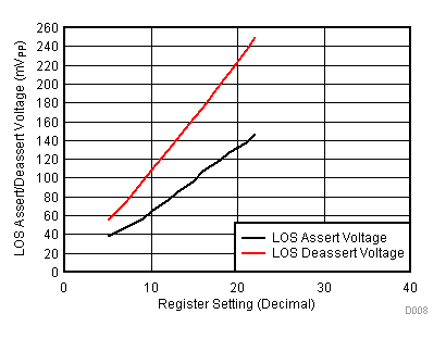
| VTH | LOW LOS assert threshold range min | PRBS7 pattern at 11.3Gbps, RXLOSRNG = 1 | 10 | mVPP | ||
| LOW LOS assert threshold range max | PRBS7 pattern at 11.3Gbps, RXLOSRNG = 1 | 50 | ||||
| VTH | HIGH LOS assert threshold range min | PRBS7 pattern at 11.3Gbps, RXLOSRNG = 0 | 40 | mVPP | ||
| HIGH LOS assert threshold range max | PRBS7 pattern at 11.3Gbps, RXLOSRNG = 0 | 130 | ||||
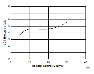
| LOS hysteresis (electrical) | 2 | 4 | 6 | dB | ||
| LOS threshold variation | Versus temperature | 1.5 | dB | |||
| Versus supply voltage | 1 | |||||
| Versus data rate | 1.5 | |||||
7.8 Timing Requirements
Over recommended operating conditions, open loop operation, TXOUT+ = 2 VPP singled-ended, I(BIAS) = 80 mA, VOD = 600 mVPP differential (unless otherwise noted). Typical operating condition is at VCC = 2.5 V and TA = 25°C| MIN | TYP | MAX | UNIT | |||
|---|---|---|---|---|---|---|
| t(APC) | APC time constant | CAPC 0.01 µF, IPD = 500 µA, PD coupling ratio CR = 150, PDRNG = 01 |
50 | µs | ||
| t(INIT1) | Power-on to initialize | Power-on to registers ready to be loaded | 0.2 | 1 | ms | |
| t(INIT2) | Initialize to transmit | Register load STOP command to part ready to transmit valid data | 2 | ms | ||
| t(OFF) | Transmitter disable time | Rising edge of TX_DIS to I(BIAS) ≤ 0.1 × I(BIAS-NOMINAL) | 1 | 5 | µs | |
| t(ON) | Disable negate time | Falling edge of TX_DIS to I(BIAS) ≥ 0.9 × I(BIAS-NOMINAL) | 1 | ms | ||
| t(RESET) | TX_DIS pulse width | Time TX_DIS must held high to reset part | 100 | ns | ||
| t(FAULT) | Fault assert time | Time from fault condition to FLT high | 50 | µs | ||
| TX OUTPUT SPECIFICATIONS in SINGLE-ENDED MODE of OPERATION (TXMODE = 1) | ||||||
| tR(OUTTX) | Output rise time | 20% - 80%, AC Coupled Outputs, 50-Ω load, single-ended | 30 | 42 | ps | |
| tF(OUTTX) | Output fall time | 20% - 80%, AC Coupled Outputs, 50-Ω load, single-ended | 30 | 42 | ps | |
| ISI(TX) | Intersymbol interference | TXEQ_DIS = 1, 11.3 Gbps, PRBS9 pattern, 150-mVpp, 600-mVpp, 1200-mVpp differential input voltage |
4 | 12 | ps | |
| TXEQ_DIS = 0, 11.3 Gbps, PRBS9 pattern, 150-mVpp, 600-mVpp, 1200-mVpp differential input voltage, maximum equalization with 18-inch transmission line at the input. |
7 | |||||
| R(J_TX) | Serial data output random jitter | 0.4 | 1 | psRMS | ||
| Output de-emphasis width | TXPKSEL = 0 | 28 | ps | |||
| TXPKSEL = 1 | 35 | |||||
| TX OUTPUT SPECIFICATIONS in DIFFERENTIAL MODE of OPERATION (TXMODE = 0) | ||||||
| tR(OUTTX) | Output rise time | 20%–80%, AC Coupled Outputs, 100-Ω differential load | 30 | 42 | ps | |
| tF(OUTTX) | Output fall time | 20%–80%, AC Coupled Outputs, 100-Ω differential load | 30 | 42 | ps | |
| ISI(TX) | Intersymbol interference | TXEQ_DIS = 1, 11.3 Gbps, PRBS9 pattern, 150-mVpp, 600-mVpp, 1200-mVpp differential input voltage |
4 | 10 | ps | |
| TXEQ_DIS = 0, 11.3 Gbps, PRBS9 pattern, 150-mVpp, 600-mVpp, 1200-mVpp differential input voltage, maximum equalization with 18-inch transmission line at the input. |
7 | |||||
| R(J_TX) | Serial data output random jitter | 0.4 | 1 | psRMS | ||
| Output Peaking Width | TXPKSEL = 0 | 28 | ps | |||
| TXPKSEL = 1 | 35 | |||||
| RX OUTPUT SPECIFICATIONS | ||||||
| tR(OUTRX) | Output rise time | 20%–80%, 100-Ω differential load, adjustable | 30 | 40 | ps | |
| tF(OUTRX) | Output fall time | 20%–80%, 100-Ω differential load, adjustable | 30 | 40 | ps | |
| Serial data output deterministic jitter | PRBS9 pattern 11.3 Gbps, VIN = 15 mVpp to 900 mVpp | 3 | 10 | ps | ||
| RX LOS SPECIFICATIONS | ||||||
| t(LOS_AST) | LOS assert time | 2.5 | 10 | 50 | μs | |
| t(LOS, DEA) | LOS deassert time | 2.5 | 10 | 50 | μs | |
 Figure 1. 2-Wire Interface Diagram
Table 1. Timing Diagram Definitions
| Symbol | Description | Min | Max | Unit |
|---|---|---|---|---|
| fSCK | SCK clock frequency | 400 | kHz | |
| tBUF | Bus free time between START and STOP conditions | 1.3 | µs | |
| tHDSTA | Hold time after repeated START condition. After this period, the first clock pulse is generated | 0.6 | µs | |
| tLOW | Low period of the SCK clock | 1.3 | µs | |
| tHIGH | High period of the SCK clock | 0.6 | µs | |
| tSUSTA | Setup time for a repeated START condition | 0.6 | µs | |
| tHDDAT | Data HOLD time | 0 | µs | |
| tSUDAT | Data setup time | 100 | ns | |
| tR | Rise time of both SDA and SCK signals | 300 | ns | |
| tF | Fall time of both SDA and SCK signals | 300 | ns | |
| tSUSTO | Setup time for STOP condition | 0.6 | µs |
7.9 Typical Characteristics
Typical operating condition is at VCC = 2.5 V, TA = 25°C, TXOUT+ = 2 VPP Single-ended, RXOUT = 600 mVPP differential, TXIN = 600 mVPP differential (unless otherwise noted).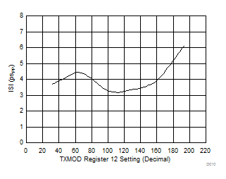
| TXMODE = 0 |
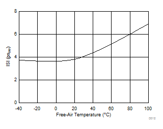
| TXMODE = 0 |
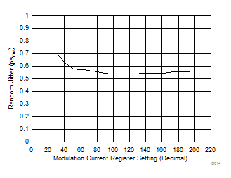
| TXMODE = 1 |
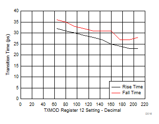
| TXMODE = 1 |
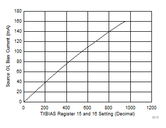
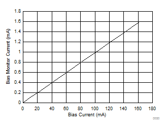
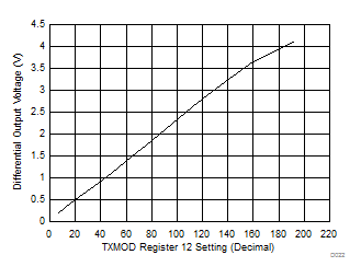
| TXMODE = 0 |
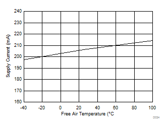
| TXMODE = 0 | Bias Current = 0 |
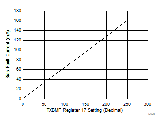
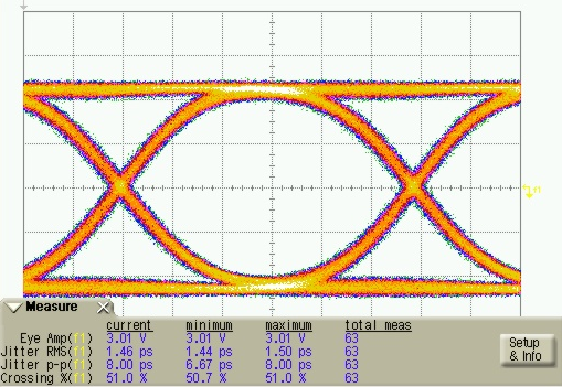
| TXMODE = 0 | 15 ps/Div |
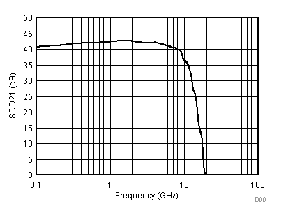
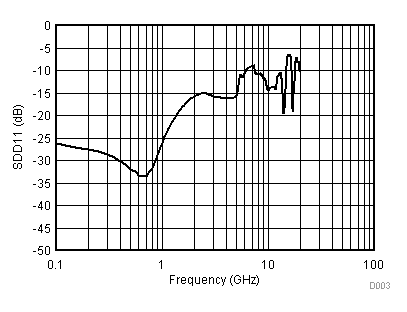
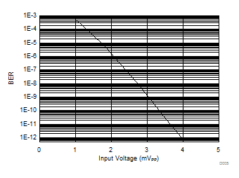
| 11.3 Gbps | TX Disabled |
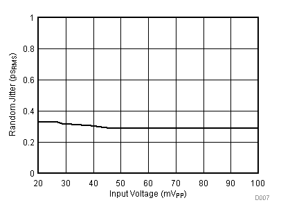
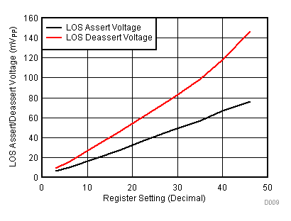
| RX LOSRNG = 1 |
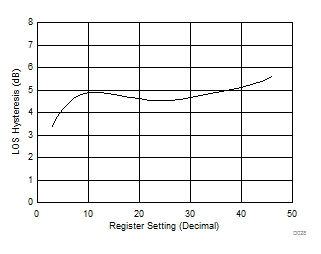
| RX LOSRNG = 1 |
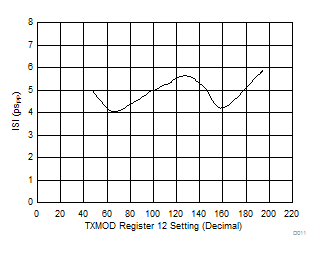
| TXMODE = 1 |
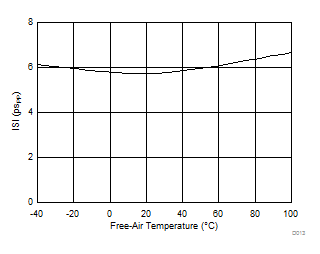
| TXMODE = 1 |
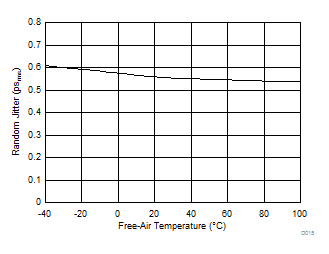
| TXMODE = 1 |
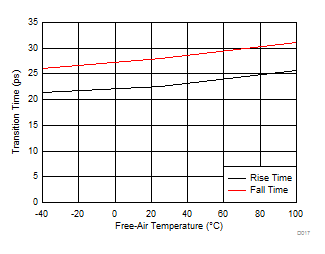
| TXMODE = 1 |
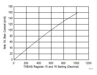
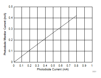
| TXPDRNG[0..1] = 00 |
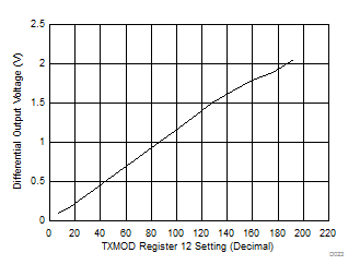
| TXMODE = 1 |
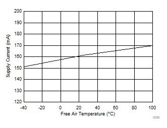
| TXMODE = 1 | Bias Current = 0 |
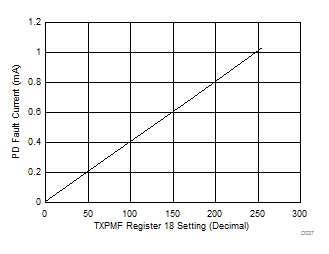
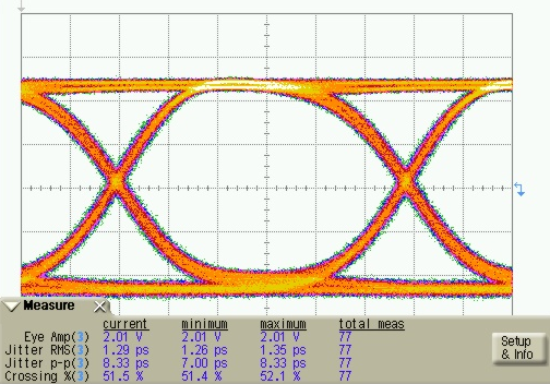
| TXMODE = 1 | 15 ps/Div |
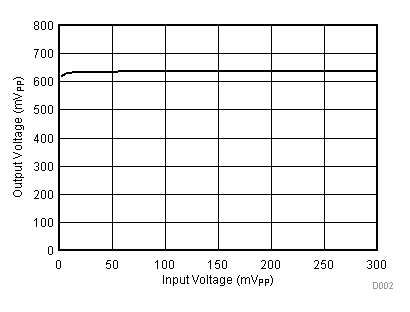
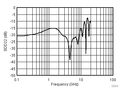
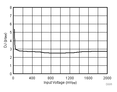
| RX LOSRNG = 0 |
| RX LOSRNG = 0 |
| VI = 20 mVPP | ||