SBOSA00B December 2019 – August 2020 OPA1637
PRODUCTION DATA
- 1 Features
- 2 Applications
- 3 Description
- 4 Revision History
- 5 Pin Configuration and Functions
- 6 Specifications
- 7 Parameter Measurement Information
- 8 Detailed Description
- 9 Application and Implementation
- 10Power Supply Recommendations
- 11Layout
- 12Device and Documentation Support
- 13Mechanical, Packaging, and Orderable Information
Package Options
Mechanical Data (Package|Pins)
- DGK|8
Thermal pad, mechanical data (Package|Pins)
- DGK|8
Orderable Information
9.1.4 Noise Performance
The first step in the output noise analysis is to reduce the application circuit to the simplest form with equal feedback and gain setting elements to ground. Figure 9-4 shows the simplest analysis circuit with the FDA and resistor noise terms to be considered.
 Figure 9-4 FDA Noise Analysis Circuit
The noise powers are shown in Figure 9-4 for each term. When the RF and RG (or RI) terms are matched on each side, the total differential output noise is the root sum squared (RSS) of these separate terms. Using NG ≡ 1 + RF / RG, the total output noise is given by Equation 3. Each resistor noise term is a 4kT × R power (4kT = 1.6E-20 J at 290 K).
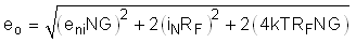
The first term is simply the differential input spot noise times the noise gain. The second term is the input current noise terms times the feedback resistor (and because there are two uncorrelated current noise terms, the power is two times one of them). The last term is the output noise resulting from both the RF and RG resistors, at again, twice the value for the output noise power of each side added together. Running a wide sweep of gains when holding RF to 2 kΩ gives the standard values and resulting noise listed in Table 9-1. When the gain increases, the input-referred noise approaches only the gain of the FDA input voltage noise term at 3.7 nV/√ Hz.
| GAIN (V/V) | RF (Ω) | RG1 (Ω) | AV | EO (nV/√ Hz) | EI (nV/√ Hz) |
|---|---|---|---|---|---|
| 0.1 | 2000 | 20000 | 0.1 | 9.4 | 93.9 |
| 1 | 2000 | 2000 | 1 | 13.6 | 13.6 |
| 2 | 2000 | 1000 | 2 | 17.8 | 8.9 |
| 5 | 2000 | 402 | 4.98 | 29.5 | 5.9 |
| 10 | 2000 | 200 | 10 | 48.6 | 4.9 |