SBOS901C March   2019  – September 2022 OPA1655 , OPA1656

PRODUCTION DATA  

  1. Features
  2. Applications
  3. Description
  4. Revision History
  5. Pin Configuration and Functions
  6. Specifications
    1. 6.1 Absolute Maximum Ratings
    2. 6.2 ESD Ratings
    3. 6.3 Recommended Operating Conditions
    4. 6.4 Thermal Information: OPA1655
    5. 6.5 Thermal Information: OPA1656
    6. 6.6 Electrical Characteristics
    7. 6.7 Typical Characteristics
  7. Detailed Description
    1. 7.1 Overview
    2. 7.2 Functional Block Diagram
    3. 7.3 Feature Description
      1. 7.3.1 Phase Reversal Protection
      2. 7.3.2 Electrical Overstress
      3. 7.3.3 EMI Rejection Ratio (EMIRR)
        1. 7.3.3.1 EMIRR IN+ Test Configuration
    4. 7.4 Device Functional Modes
  8. Application and Implementation
    1. 8.1 Application Information
      1. 8.1.1 Basic Noise Calculations
    2. 8.2 Typical Applications
      1. 8.2.1 Preamplifier Circuit for Vinyl Record Playback With Moving-Magnet Phono Cartridges
        1. 8.2.1.1 Design Requirements
        2. 8.2.1.2 Detailed Design Procedure
        3. 8.2.1.3 Application Curves
      2. 8.2.2 Composite Headphone Amplifier
        1. 8.2.2.1 Application Curves
      3. 8.2.3 Baxandall Tone Control
        1. 8.2.3.1 Application Curves
      4. 8.2.4 Guitar Input to XLR Output
        1. 8.2.4.1 Application Curves
    3. 8.3 Power Supply Recommendations
    4. 8.4 Layout
      1. 8.4.1 Layout Guidelines
        1. 8.4.1.1 Power Dissipation
      2. 8.4.2 Layout Example
  9. Device and Documentation Support
    1. 9.1 Device Support
      1. 9.1.1 Development Support
        1. 9.1.1.1 PSpice® for TI
        2. 9.1.1.2 TINA-TI™ Simulation Software (Free Download)
        3. 9.1.1.3 DIP-Adapter-EVM
        4. 9.1.1.4 DIYAMP-EVM
        5. 9.1.1.5 TI Reference Designs
        6. 9.1.1.6 Filter Design Tool
    2. 9.2 Documentation Support
      1. 9.2.1 Related Documentation
    3. 9.3 Receiving Notification of Documentation Updates
    4. 9.4 Support Resources
    5. 9.5 Trademarks
    6. 9.6 Electrostatic Discharge Caution
    7. 9.7 Glossary
  10. 10Mechanical, Packaging, and Orderable Information

Package Options

Mechanical Data (Package|Pins)
Thermal pad, mechanical data (Package|Pins)
Orderable Information

Typical Characteristics

at TA = 25°C, VS = ±15 V, RL = 2 kΩ, and VCM = VS/2 (unless otherwise noted)
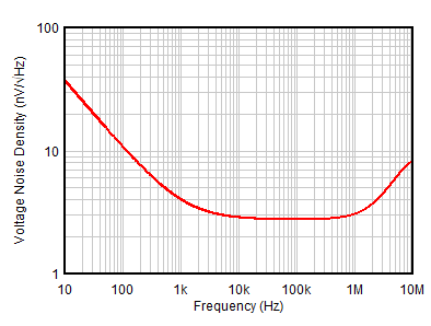
GUID-47DF38E8-1957-4576-B54A-2324446A2835-low.gif
 
Figure 6-1 Input Voltage Noise Density vs Frequency
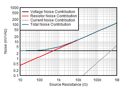
GUID-938DF980-67BC-4953-8978-45DDFDFB22DA-low.gif
 
Figure 6-3 Voltage Noise vs Source Resistance
GUID-B0C341F5-317A-4A52-9320-C1911903EB86-low.gif
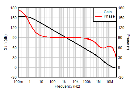
CL = 10 pF
Figure 6-5 Open-Loop Gain and Phase vs Frequency
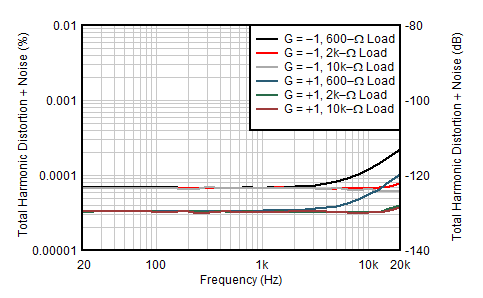
GUID-C1BFD5CB-EE45-4B3A-B965-3242281284CB-low.gif
VOUT = 3 VRMSBandwidth = 80 kHz
Figure 6-7 THD+N Ratio vs Frequency
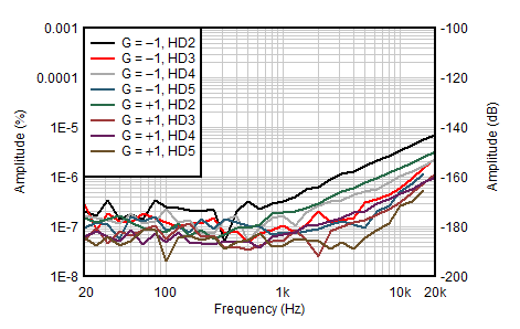
GUID-8E0BDF1C-5141-4846-8514-574D84EFBCA9-low.gif
VOUT = 3 VRMSBandwidth = 80 kHz
Figure 6-9 Individual Harmonic Amplitude vs Frequency
GUID-FCF39615-1317-4438-8FEF-86082DA81B37-low.gif
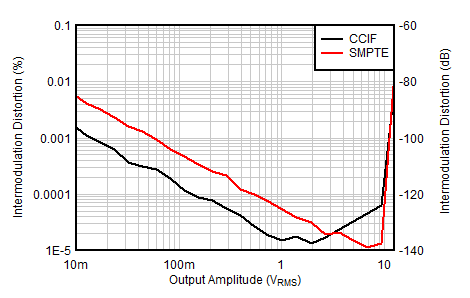
Bandwidth = 80 kHz
Figure 6-11 Intermodulation Distortion vs Amplitude
GUID-769372D9-29F6-4F9F-9468-89A44B7D27F9-low.gif
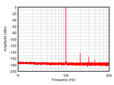
G = 1, VOUT = 3 VRMSRL = 2 kΩBandwidth = 80 kHz
Figure 6-13 FFT, 10-kHz Sine Wave
GUID-D2E90CAA-6A88-4F24-990E-24FFBF971AC2-low.gif
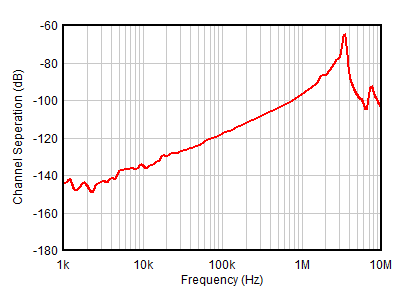
VOUT = 3 VRMSG = 1
Figure 6-15 Channel Separation vs Frequency
GUID-1870A755-3729-4914-B227-A70BE06C0DBD-low.gif
 
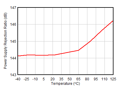
Figure 6-17 Power Supply Rejection Ratio vs Temperature (Referred to Input)
GUID-87DCD854-93B9-468E-A9EC-390812684A4D-low.gif
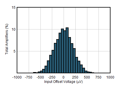
Count = 7955
Figure 6-19 Input Offset Voltage Distribution
GUID-39271F3A-464E-4498-9407-DC70FBB1D7F7-low.gif
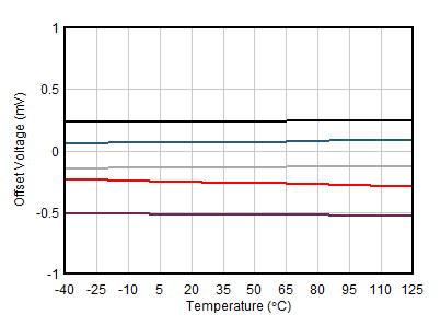
5 typical units shown
Figure 6-21 Input Offset vs Temperature
GUID-ADADDD50-7B09-44DD-A1D0-0B3CEF3D4533-low.gif
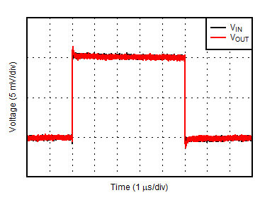
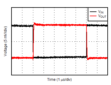
G = 1CL = 20 pF
Figure 6-23 Small-Signal Step Response (100 mV)
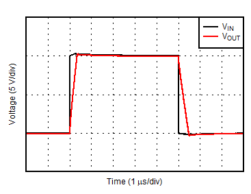
GUID-B047540A-A92C-4801-80DA-D4121A8A0CCB-low.gif
G = 1RL = 2 kΩCL = 100 pF
Figure 6-25 Large-Signal Step Response
GUID-C6CBD202-94B5-443B-8F23-F919733768C9-low.gif
 
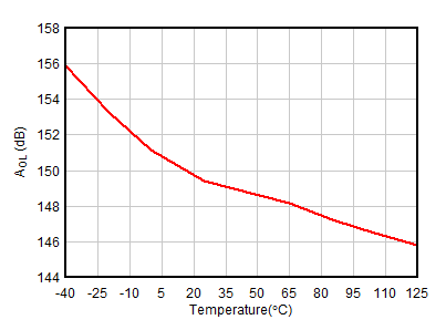
Figure 6-27 Open-Loop Gain vs Temperature
GUID-A6FB231A-AD16-4E15-8700-2284C3E8068A-low.gif
 
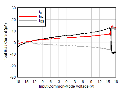
Figure 6-29 IB and IOS vs Common-Mode Voltage
GUID-6371B997-C392-47AB-B6EA-64B1079296EA-low.gif
 
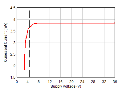
Figure 6-31 Supply Current vs Supply Voltage
GUID-E7291C88-E381-4FAB-99FE-D013B48D11AA-low.gif
 
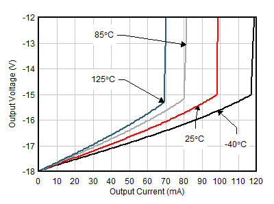
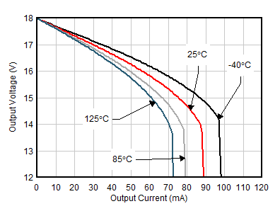
Figure 6-33 Output Voltage vs Output Current (Sinking)
GUID-607AE3D5-A5AD-4BDF-8251-B617CD3FB37B-low.gif
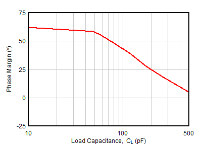
G = 1
Figure 6-35 Phase Margin vs Capacitive Load
GUID-0EA53B19-9726-4991-8951-DE6DC9FD7FCA-low.gif
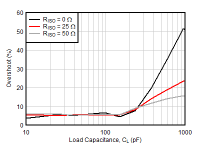
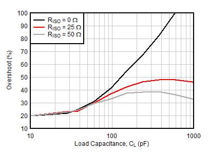
G = –1
Figure 6-37 Percent Overshoot vs Capacitive Load
GUID-30C01021-9E69-43D4-982A-C292A39377AE-low.gif
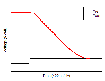
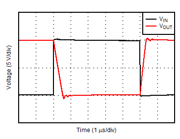
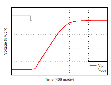
G = –10
Figure 6-39 Positive Overload Recovery
GUID-30C01021-9E69-43D4-982A-C292A39377AE-low.gif
G = 1
Figure 6-41 No Phase Reversal
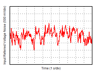
GUID-1DD46EE4-B54D-4253-8A26-D55D75C3E129-low.gif
 
Figure 6-2 0.1-Hz to 10-Hz Noise
GUID-F29B3673-F5C2-4550-AF5E-0BBDF1DABFFE-low.gif
 
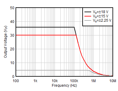
Figure 6-4 Maximum Output Voltage vs Frequency
GUID-B53990A3-1628-41CE-B7F5-5243AF85DCF6-low.gif
 CL = 10 pF
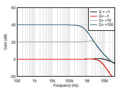
Figure 6-6 Closed-Loop Gain vs Frequency
GUID-240ADD34-A559-478C-A2F2-A3AE40EF91C4-low.gif
f = 1 kHzBandwidth = 80 kHz
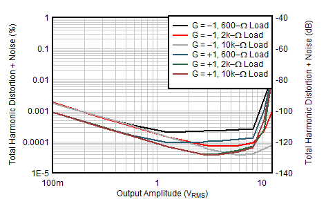
Figure 6-8 THD+N Ratio vs Output Amplitude
GUID-E11B64A0-2C25-4F9C-8E7D-CA4B810245D7-low.gif
f = 1 kHzRL = 2 kΩBandwidth = 80 kHz
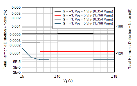
Figure 6-10 THD+N vs Supply Voltage
GUID-3C183184-8961-43B2-86B3-3724165755CB-low.gif
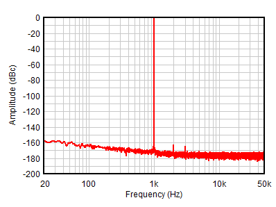
G = 1, VOUT = 3 VRMSRL = 2 kΩBandwidth = 80 kHz
Figure 6-12 FFT, 1-kHz Sine Wave
GUID-94D94D80-6032-4161-8425-2B4BD6916EF1-low.gif
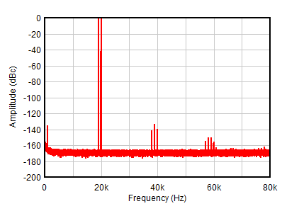
VOUT = 3 VRMSRL = 2 kΩBandwidth = 80 kHz
Figure 6-14 FFT, CCIF Input (19 kHz + 20 kHz)
GUID-06B45952-C5EA-4EB9-8FC9-05303D2231B7-low.gif
 
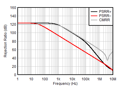
Figure 6-16 CMRR and PSRR vs Frequency (Referred to Input)
GUID-6F7C22A1-6F6A-42C2-8A00-4F4DCCBC3E91-low.gif
 
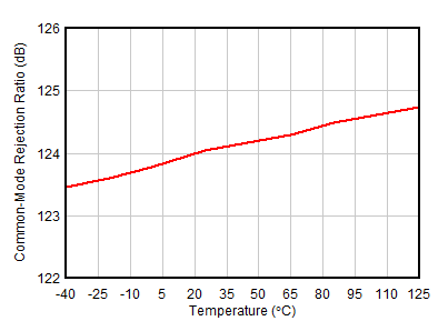
Figure 6-18 Common Mode Rejection Ratio vs Temperature (Referred to Input)
GUID-4635FA55-79A3-4B09-9561-31D89D899ECA-low.gif
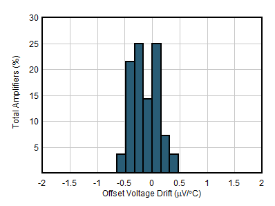
Count = 32
Figure 6-20 Input Offset Voltage Drift Distribution
GUID-7326D0FC-AAB4-4F8D-9EC1-0B9848C5A575-low.gif
 
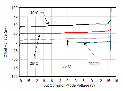
Figure 6-22 Input Offset vs Common Mode Voltage
GUID-AC605CB9-6C8C-42C2-B200-509C38A94432-low.gif
G = –1CL = 100 pF
Figure 6-24 Small-Signal Step Response (100 mV)
GUID-623DC51B-D072-4DAF-A355-6E7F85F5AE32-low.gif
G = –1CL = 100 pF
Figure 6-26 Large-Signal Step Response
GUID-361034D2-8C01-4643-9A14-C5AE9AC726D1-low.gif
 
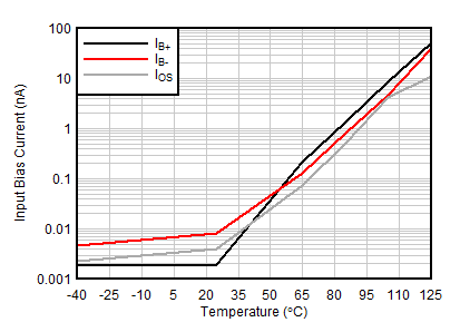
Figure 6-28 IB and IOS vs Temperature
GUID-C7452BEE-CB3C-4357-AA34-6E703AC148EB-low.gif
 
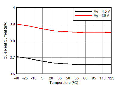
Figure 6-30 Supply Current vs Temperature
GUID-6112BB46-035F-4DF5-BB2B-6148A5A7133F-low.gif
 
Figure 6-32 Output Voltage vs Output Current (Sourcing)
GUID-6647E43B-C682-4D83-A369-30AEA369EC56-low.gif
 
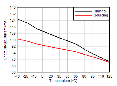
Figure 6-34 Short-Circuit Current vs Temperature
GUID-6E7349D0-6E39-46D6-8318-8F6457C06B40-low.gif
G = 1
Figure 6-36 Percent Overshoot vs Capacitive Load
GUID-C6B7A49A-1402-40DD-926A-8F4AF5A17483-low.gif
G = –10
Figure 6-38 Negative Overload Recovery
GUID-02CC1AE7-BC60-443D-ACD8-0C60AF1ED501-low.gif
 
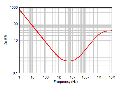
Figure 6-40 Open-Loop Output Impedance vs Frequency