SBOS618I December   2013  – May 2018 OPA172 , OPA2172 , OPA4172

PRODUCTION DATA.  

  1. Features
  2. Applications
  3. Description
    1.     Device Images
      1.      JFET-Input Low-Noise Amplifier
      2.      Superior THD Performance
  4. Revision History
  5. Device Comparison
    1. 5.1 Device Comparison
    2. 5.2 Device Family Comparison
  6. Pin Configuration and Functions
    1.     Pin Functions: OPA172
    2.     Pin Functions: OPA2172 and OPA4172
  7. Specifications
    1. 7.1 Absolute Maximum Ratings
    2. 7.2 ESD Ratings
    3. 7.3 Recommended Operating Conditions
    4. 7.4 Thermal Information: OPA172
    5. 7.5 Thermal Information: OPA2172
    6. 7.6 Thermal Information: OPA4172
    7. 7.7 Electrical Characteristics
    8. 7.8 Typical Characteristics: Table of Graphs
    9. 7.9 Typical Characteristics
  8. Detailed Description
    1. 8.1 Overview
    2. 8.2 Functional Block Diagram
    3. 8.3 Feature Description
      1. 8.3.1 EMI Rejection
      2. 8.3.2 Phase-Reversal Protection
      3. 8.3.3 Capacitive Load and Stability
    4. 8.4 Device Functional Modes
      1. 8.4.1 Common-Mode Voltage Range
      2. 8.4.2 Electrical Overstress
      3. 8.4.3 Overload Recovery
  9. Applications and Implementation
    1. 9.1 Application Information
    2. 9.2 Typical Applications
      1. 9.2.1 Capacitive Load Drive Solution Using an Isolation Resistor
        1. 9.2.1.1 Design Requirements
        2. 9.2.1.2 Detailed Design Procedure
        3. 9.2.1.3 Application Curve
      2. 9.2.2 Bidirectional Current Source
      3. 9.2.3 JFET-Input Low-Noise Amplifier
  10. 10Power-Supply Recommendations
  11. 11Layout
    1. 11.1 Layout Guidelines
    2. 11.2 Layout Example
  12. 12Device and Documentation Support
    1. 12.1 Device Support
      1. 12.1.1 Development Support
        1. 12.1.1.1 TINA-TI (Free Software Download)
    2. 12.2 Documentation Support
      1. 12.2.1 Related Documentation
    3. 12.3 Related Links
    4. 12.4 Community Resources
    5. 12.5 Trademarks
    6. 12.6 Electrostatic Discharge Caution
    7. 12.7 Glossary
  13. 13Mechanical, Packaging, and Orderable Information

Package Options

Mechanical Data (Package|Pins)
Thermal pad, mechanical data (Package|Pins)
Orderable Information

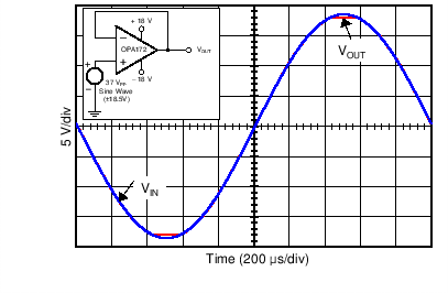
Phase-Reversal Protection

The OPAx172 family has internal phase-reversal protection. Many op amps exhibit a phase reversal when the input is driven beyond the linear common-mode range. This condition is most often encountered in noninverting circuits when the input is driven beyond the specified common-mode voltage range, causing the output to reverse into the opposite rail. The input of the OPAx172 prevents phase reversal with excessive common-mode voltage. Instead, the appropriate rail limits the output voltage. This performance is shown in Figure 43.
OPA172 OPA2172 OPA4172 C014_SBOS618.pngFigure 43. No Phase Reversal