SBOS830I September 2017 – October 2021 OPA189 , OPA2189 , OPA4189
PRODUCTION DATA
- 1 Features
- 2 Applications
- 3 Description
- 4 Revision History
- 5 Device Comparison Table
- 6 Pin Configuration and Functions
- 7 Specifications
- 8 Detailed Description
- 9 Application and Implementation
- 10Power Supply Recommendations
- 11Layout
- 12Device and Documentation Support
- 13Mechanical, Packaging, and Orderable Information
Package Options
Mechanical Data (Package|Pins)
Thermal pad, mechanical data (Package|Pins)
- DGK|8
Orderable Information
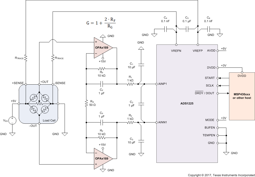
9.3.1 24-Bit, Delta-Sigma, Differential Load Cell or Strain Gauge Sensor Signal Conditioning
OPAx189 is used in a 24-bit, differential load cell or strain gauge sensor signal conditioning system alongside the ADS1225. A pair of OPAx189 amplifiers are configured in a two-amp instrumentation amplifier (IA) configuration and are band-limited to reduce noise and allow heavy capacitive drive. The load cell is powered by an excitation voltage (denoted VEX) of 5-V and provides a differential voltage proportional to force applied. The differential voltage can be quite small and both outputs are biased to VEX / 2.
In this example the OPAx189 is employed here due to the excellent input offset voltage (0.4 µV) and input offset voltage drift (0.005 µV/°C), the low broadband noise (5.2 nV/√ Hz) and zero-flicker noise, and excellent linearity and high input impedance. The two-amp IA configuration removes the dc bias and amplifies the differential signal of interest and drives the 24-bit, delta-sigma ADS1225 analog-to-digital converter (ADC) for acquisition and conversion. The ADS1225 features a 100-SPS data rate, single-cycle settling, and simple conversion control with the dedicated START pin.
 Figure 9-8 24-Bit, Differential Load Cell or Strain Gauge Sensor Signal Conditioning Schematic