SBOS620E December 2013 – November 2015 OPA192 , OPA2192 , OPA4192
PRODUCTION DATA.
- 1 Features
- 2 Applications
- 3 Description
- 4 Revision History
- 5 Pin Configuration and Functions
-
6 Specifications
- 6.1 Absolute Maximum Ratings
- 6.2 ESD Ratings
- 6.3 Recommended Operating Conditions
- 6.4 Thermal Information: OPA192
- 6.5 Thermal Information: OPA2192
- 6.6 Thermal Information: OPA4192
- 6.7 Electrical Characteristics: VS = ±4 V to ±18 V (VS = +8 V to +36 V)
- 6.8 Electrical Characteristics: VS = ±2.25 V to ±4 V (VS = +4.5 V to +8 V)
- 6.9 Typical Characteristics
- 6.10 Typical Characteristics
- 7 Parameter Measurement Information
- 8 Detailed Description
- 9 Application and Implementation
- 10Power-Supply Recommendations
- 11Layout
- 12Device and Documentation Support
- 13Mechanical, Packaging, and Orderable Information
Package Options
Mechanical Data (Package|Pins)
Thermal pad, mechanical data (Package|Pins)
Orderable Information
7 Parameter Measurement Information
7.1 Input Offset Voltage Drift
The OPAx192 family of operational amplifiers is manufactured using TI’s e-trim technology. Each amplifier input offset voltage and input offset voltage drift is trimmed in production, thereby minimizing errors associated with input offset voltage and input offset voltage drift. The e-trim technology is a TI proprietary method of trimming internal device parameters during either wafer probing or final testing. When trimming input offset voltage drift the systematic or linear drift error on each device is trimmed to zero. This results in the remaining errors associated with input offset drift are minimal and are the result from only nonlinear error sources. Figure 49 illustrates this concept.
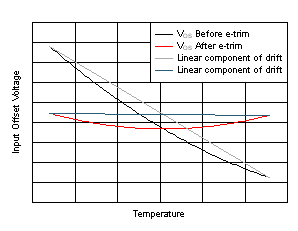 Figure 49. Input Offset Before and After Drift Trim
A common method of specifying input offset voltage drift is the box method. The box method estimates a maximum input offset drift by bounding the offset voltage versus temperature curve with a box and using the corners of this bounding box to determine the drift. The slope of the line connecting the diagonal corners of the box corresponds to the input offset voltage drift. Figure 50 shows the box method concept. The box method works particularly well when the input offset drift is dominated by the linear component of drift, but because the OPA192 family uses TI’s e-trim technology to remove the linear component input offset voltage drift, the box method is not a particularly useful method of accurately performing an error analysis. Figure 50 shows 30 typical units of the OPAx192 with the box method superimposed for illustrative purposes. The boundaries of the box are determined by the specified temperature range along the x-axis and the maximum specified input offset voltage across that same temperature range along the y-axis. Using the box method predicts an input offset voltage drift of 0.9 µV/°C. As shown in Figure 50, the slopes of the actual input offset voltage versus temperature are much less than that predicted by the box method. The box method predicts a pessimistic value for the maximum input offset voltage drift and is not recommended when performing an error analysis.
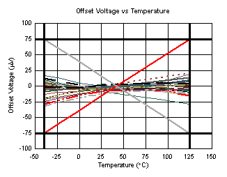 Figure 50. The Box Method
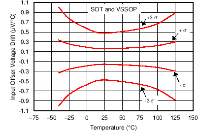
Instead of the box method, a convenient way to illustrate input offset drift is to compute the slopes of the input offset voltage versus temperature curve. This is the same as computing the input offset drift at each point along the input offset voltage versus temperature curve. The results for the OPAx192 family are shown in Figure 51 and Figure 52.
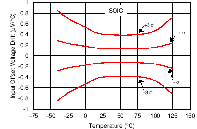 Figure 51. Input Offset Voltage Drift vs Temperature
(OPA192ID and OPA2192ID)
As shown in Figure 51, the input offset drift is typically less than ±0.3 µV/°C over the range from –40°C to +125°C. When performing an error analysis over the full specified temperature range, use the typical and maximum values for input offset voltage drift as described in the Electrical Characteristics tables. If a reduced temperature range is applicable, use the information shown in Figure 51 or Figure 52 when performing an error analysis. To determine the change in input offset voltage, use Equation 1:
where
- ΔVOS = Change in input offset voltage
- ΔT = Change in temperature
- dVOS/dT = Input offset voltage drift
For example, determine the amount of OPA192ID input offset voltage change over the temperature range of 25°C to 75°C for 1 σ (68%) of the units. As shown in Figure 51, the input offset drift is typically 0.15 µV/°C. This input offset drift results in a typical input offset voltage change of (75°C – 25°C) × 0.15 µV/°C = 7.5 µV .
For 3 σ (99.7%) of the units, Figure 51 shows a typical input offset drift of 0.4 µV/°C. This input offset drift results in a typical input offset voltage change of (75°C – 25°C) × 0.4 µV/°C = 20 µV.
Figure 53 shows six typical units.
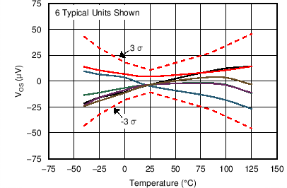 Figure 53. Input Offset Voltage Drift vs Temperature for Six Typical Units
