SBOS584E November 2011 – June 2018 OPA180 , OPA2180 , OPA4180
PRODUCTION DATA.
- 1 Features
- 2 Applications
- 3 Description
- 4 Revision History
- 5 Device Comparison Table
- 6 Pin Configuration and Functions
-
7 Specifications
- 7.1 Absolute Maximum Ratings
- 7.2 ESD Ratings
- 7.3 Recommended Operating Conditions
- 7.4 Thermal Information: OPA180
- 7.5 Thermal Information: OPA2180
- 7.6 Thermal Information: OPA4180
- 7.7 Electrical Characteristics: VS = ±2 V to ±18 V (VS = 4 V to 36 V)
- 7.8 Typical Characteristics: Table of Graphs
- 7.9 Typical Characteristics
- 8 Detailed Description
- 9 Application and Implementation
- 10Power Supply Recommendations
- 11Layout
- 12Device and Documentation Support
- 13Mechanical, Packaging, and Orderable Information
Package Options
Mechanical Data (Package|Pins)
Thermal pad, mechanical data (Package|Pins)
Orderable Information
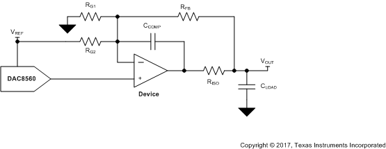
9.2.1 Bipolar ±10-V Analog Output from a Unipolar Voltage Output DAC
This design is used for conditioning a unipolar digital-to-analog converter (DAC) into an accurate bipolar signal source using the OPAx180 family and three resistors. The circuit is designed with reactive load stability in mind, and is compensated to drive nearly any conventional capacitive load associated with long cable lengths.
 Figure 30. Circuit Schematic