SBOSA11E March 2020 – December 2023 OPA206 , OPA2206 , OPA4206
PRODUCTION DATA
- 1
- 1 Features
- 2 Applications
- 3 Description
- 4 Pin Configuration and Functions
- 5 Specifications
- 6 Parameter Measurement Information
- 7 Detailed Description
- 8 Application and Implementation
- 9 Device and Documentation Support
- 10Revision History
- 11Mechanical, Packaging, and Orderable Information
Package Options
Refer to the PDF data sheet for device specific package drawings
Mechanical Data (Package|Pins)
- D|8
- DGK|8
Thermal pad, mechanical data (Package|Pins)
Orderable Information
7.3.3 Lower Input Bias With Super-Beta Inputs
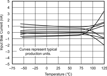
The OPAx206 have a super-beta input transistor architecture. In a transistor, the beta value is the ratio between the current flowing into the base and the current flowing from the collector to the emitter. A super-beta transistor is one where the beta value has been increased from several hundred to thousands. In a bipolar amplifier, the input bias current is the current flowing into the base of the input transistor pair, as well as a small leakage current that flows through the ESD diodes. A super-beta input reduces the input bias current of the amplifier. In addition, the super-beta inputs lower the input current noise that is directly related to the input bias current of the device. A comparison between the input bias current of the OPA2277 and the OPAx206 super-beta input bias currents can be seen in Figure 7-6 and Figure 7-7.
 Figure 7-6 OPA2277 Input Bias
Current
 Figure 7-7 OPAx206 Super-Beta Input Bias Current