SBOS377L October   2006  – January 2020 OPA211

PRODUCTION DATA.  

  1. Features
  2. Applications
  3. Description
    1.     Device Images
      1.      Input Voltage Noise Density vs Frequency
  4. Revision History
  5. Pin Configuration and Functions
    1.     Pin Functions: OPA211
    2.     Pin Functions: OPA2211
  6. Specifications
    1. 6.1 Absolute Maximum Ratings
    2. 6.2 ESD Ratings
    3. 6.3 Recommended Operating Conditions
    4. 6.4 Thermal Information: OPA211 and OPA211A
    5. 6.5 Thermal Information: OPA2211 and OPA2211A
    6. 6.6 Electrical Characteristics: Standard Grade OPAx211A
    7. 6.7 Electrical Characteristics: High-Grade OPAx211
    8. 6.8 Typical Characteristics
  7. Detailed Description
    1. 7.1 Overview
    2. 7.2 Functional Block Diagram
    3. 7.3 Feature Description
      1. 7.3.1 Total Harmonic Distortion Measurements
    4. 7.4 Device Functional Modes
      1. 7.4.1 Shutdown
  8. Application and Implementation
    1. 8.1 Application Information
      1. 8.1.1 Operating Voltage
      2. 8.1.2 Input Protection
      3. 8.1.3 Noise Performance
      4. 8.1.4 Basic Noise Calculations
      5. 8.1.5 EMI Rejection
      6. 8.1.6 EMIRR +IN Test Configuration
      7. 8.1.7 Electrical Overstress
    2. 8.2 Typical Application
      1. 8.2.1 Design Requirements
      2. 8.2.2 Detailed Design Procedure
      3. 8.2.3 Application Curve
  9. Power Supply Recommendations
  10. 10Layout
    1. 10.1 Layout Guidelines
      1. 10.1.1 SON Layout Guidelines
    2. 10.2 Layout Example
  11. 11Device and Documentation Support
    1. 11.1 Device Support
      1. 11.1.1 Development Support
        1. 11.1.1.1 TINA-TI™ (Free Software Download)
        2. 11.1.1.2 TI Precision Designs
        3. 11.1.1.3 WEBENCH® Filter Designer
    2. 11.2 Documentation Support
      1. 11.2.1 Related Documentation
    3. 11.3 Related Links
    4. 11.4 Receiving Notification of Documentation Updates
    5. 11.5 Support Resources
    6. 11.6 Trademarks
    7. 11.7 Electrostatic Discharge Caution
    8. 11.8 Glossary
  12. 12Mechanical, Packaging, and Orderable Information

Package Options

Mechanical Data (Package|Pins)
Thermal pad, mechanical data (Package|Pins)
Orderable Information

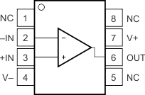
Pin Configuration and Functions

OPA211 D Package
8-Pin SOIC
Top View
OPA211 OPA2211 po_211so_bos377.gif
OPA211 DGK Package
8-Pin VSSOP
Top View
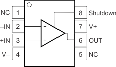
OPA211 OPA2211 po_211msop_bos377.gif
OPA211 DRG Package
8-Pin SON With Exposed Thermal Pad
Top View
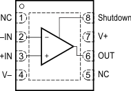
OPA211 OPA2211 po_211dfn_bos377.gif

Pin Functions: OPA211

PIN I/O DESCRIPTION
NAME NO.
+IN 3 I Noninverting input
–IN 2 I Inverting input
NC 1, 5 No internal connection. This pin can be left floating or connected to any voltage between (V–) and (V+).
OUT 6 O Output
Shutdown 8 I Shutdown, active high
The shutdown function is as follows:

Device enabled: (V–) ≤ VSHUTDOWN ≤ (V+) – 3 V


Device disabled: VSHUTDOWN ≥ (V+) – 0.35 V

V+ 7 I Positive power supply
V– 4 I Negative power supply
Thermal pad Exposed thermal die pad on underside; connect thermal die pad to V–. Soldering the thermal pad to the printed circuit board is required and improves heat dissipation and provides specified performance.
OPA2211 DRG Package
8-Pin SON With Exposed Thermal Pad
Top View
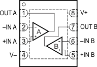
OPA211 OPA2211 po_2211dfn_bos377.gif
OPA2211 DDA Package
8-Pin SO PowerPAD With Exposed Thermal Pad
Top View
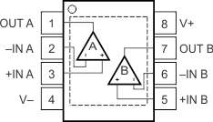
OPA211 OPA2211 po_2211so_bos377.gif

Pin Functions: OPA2211

PIN I/O DESCRIPTION
NAME NO.
+IN A 3 I Noninverting input channel A
–IN A 2 I Inverting input channel A
+IN B 5 I Noninverting input channel B
–IN B 6 I Inverting input channel B
OUT A 1 O Output channel A
OUT B 7 O Output channel B
V+ 8 I Positive power supply
V– 4 I Negative power supply
Thermal pad Exposed thermal die pad on underside; connect thermal die pad to V–. Soldering the thermal pad improves heat dissipation and provides specified performance.