SBOS110C May 1998 – March 2023 OPA2227 , OPA2228 , OPA227 , OPA228 , OPA4227 , OPA4228
PRODUCTION DATA
- 1 Features
- 2 Applications
- 3 Description
- 4 Revision History
- 5 Pin Configuration and Functions
-
6 Specifications
- 6.1 Absolute Maximum Ratings
- 6.2 ESD Ratings
- 6.3 Recommended Operating Conditions
- 6.4 Thermal Information: OPA227, OPA228
- 6.5 Thermal Information: OPA2227, OPA2228
- 6.6 Thermal Information: OPA4227, OPA4228
- 6.7 Electrical Characteristics: OPAx227
- 6.8 Electrical Characteristics: OPAx228
- 6.9 Typical Characteristics
- 7 Detailed Description
-
8 Application and Implementation
- 8.1 Application Information
- 8.2 Typical Application
- 8.3 Power Supply Recommendations
- 8.4 Layout
- 9 Device and Documentation Support
- 10Mechanical, Packaging, and Orderable Information
Package Options
Mechanical Data (Package|Pins)
Thermal pad, mechanical data (Package|Pins)
- D|8
Orderable Information
7.3.7 Basic Noise Calculations
Design of low noise operational amplifier circuits requires careful consideration of a variety of possible noise contributors: noise from the signal source, noise generated in the operational amplifier, and noise from the feedback network resistors. The total noise of the circuit is the root-sum-square combination of all noise components.
The resistive portion of the source impedance produces thermal noise proportional to the square root of the resistance. This function is shown plotted in Figure 7-4. Because the source impedance is usually fixed, select the operational amplifier and the feedback resistors to minimize any contribution to the total noise.
Figure 7-4 shows the total noise for varying source impedances with the operational amplifier in a unity-gain configuration (no feedback resistor network and therefore no additional noise contributions). The operational amplifier contributes both a voltage noise component and a current noise component. The voltage noise is commonly modeled as a time-varying component of the offset voltage. The current noise is modeled as the time-varying component of the input bias current and reacts with the source resistance to create a voltage component of noise. Consequently, the lowest noise operational amplifier for a given application depends on the source impedance. For low source impedance, current noise is negligible and voltage noise generally dominates. For high source impedance, current noise can dominate.
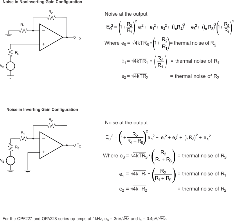
Figure 7-5 shows both inverting and noninverting operational amplifier circuit configurations with gain. In circuit configurations with gain, the feedback network resistors also contribute noise. The current noise of the operational amplifier reacts with the feedback resistors to create additional noise components. The feedback resistor values can generally be chosen to make these noise sources negligible. The equations for total noise are shown in the following images for both configurations.
 Figure 7-5 Noise Calculation in Gain Configurations
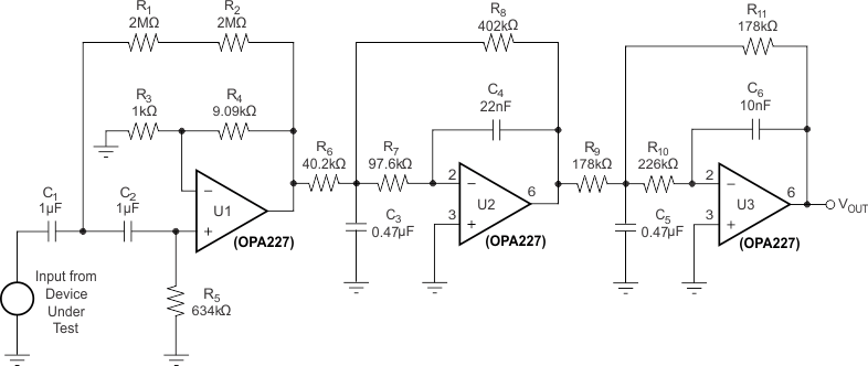
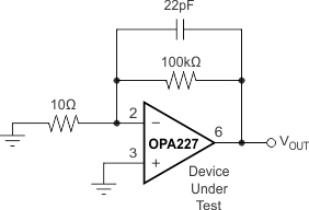
Figure 7-6 shows the 0.1 Hz 10 Hz bandpass filter used to test the noise of the OPA227 and OPA228. The filter circuit was designed using Texas Instruments’ FilterPro software (available at www.ti.com). Figure 7-7 shows the configuration of the OPA227 and OPA228 for noise testing.
 Figure 7-6 0.1 Hz to 10 Hz Bandpass Filter Used to Test Wideband Noise of the OPAx22x Series
 Figure 7-7 Noise Test Circuit