SBOS984G November 2020 – September 2023 OPA2387 , OPA387 , OPA4387
PRODUCTION DATA
- 1
- 1 Features
- 2 Applications
- 3 Description
- 4 Revision History
- 5 Pin Configuration and Functions
- 6 Specifications
- 7 Detailed Description
- 8 Application and Implementation
- 9 Device and Documentation Support
- 10Mechanical, Packaging, and Orderable Information
Package Options
Mechanical Data (Package|Pins)
Thermal pad, mechanical data (Package|Pins)
Orderable Information
7.3.2 EMI Susceptibility and Input Filtering
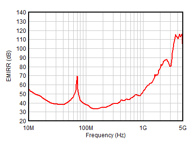
Operational amplifiers can exhibit sensitivity to electromagnetic interference (EMI). Typically, conducted EMI (that is, EMI that enters the device through conduction) is more commonly observed than radiated EMI (that is, EMI that enters the device through radiation). When conducted EMI enters the operational amplifier, the dc offset at the amplifier output can shift from the nominal value. This shift is a result of signal rectification associated with the internal semiconductor junctions. Although all operational amplifier pin functions can be affected by EMI, the input pins are likely to be the most susceptible. The OPAx387 operational amplifier family incorporates an internal input low-pass filter that reduces the amplifier response to EMI. Both common-mode and differential-mode filtering are provided by the input filter. The conducted EMI rejection of the OPAx387 is seen in Figure 7-2.
 Figure 7-2 EMI Rejection
Ratio