SBOS981J October 2019 – April 2021 OPA2607 , OPA607
PRODUCTION DATA
- 1 Features
- 2 Applications
- 3 Description
- 4 Revision History
- 5 Device Comparison
- 6 Pin Configuration and Functions
- 7 Specifications
- 8 Detailed Description
- 9 Application and Implementation
- 10Power Supply Recommendations
- 11Layout
- 12Device and Documentation Support
- 13Mechanical, Packaging, and Orderable Information
Package Options
Mechanical Data (Package|Pins)
Thermal pad, mechanical data (Package|Pins)
Orderable Information
9.2.2 Noninverting Gain of 3 V/V
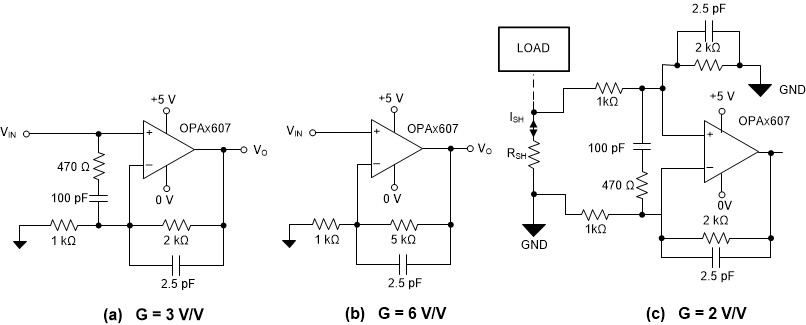
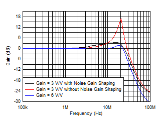
The OPAx607 devices are normally stable in noise gain configurations (see SBOA066) of greater than 6 V/V when conventional feedback networks are used, which is discussed in Section 8.3.4. The OPAx607 devices can be configured in noise gains of less than 6 V/V by using capacitors in the feedback path and between the inputs to maintain the desired gain at lower frequencies and increase the gain greater that 6 V/V at higher frequencies such that the amplifier is stable. Configuration (a) in Figure 9-6 shows OPAx607 devices configured in a gain of 3 V/V by using capacitors and resistors to shape the noise gain and achieve a phase margin of approximately 56° that is very close to the phase margin achieved for the conventional 6 V/V configuration (b) in Figure 9-6.
The key benefit of using a decompensated amplifier (such as the OPAx607) below the minimum stable gain, is that it takes advantage of the low noise and low distortion performance at quiescent powers smaller than comparable unity-gain stable architectures. By reducing the 100-pF input capacitor, higher closed-loop bandwidth can be achieved at the expense of increased peaking and reduced phase margin. Ensure that low parasitic capacitance layout techniques on the IN– pin are as small as 1 pF to 2 pF of parasitic capacitance on the inverting input, which will require tweaking the noise-shaping component values to get a flat frequency response and the desired phase margin. Configurations in Figure 9-6 does not take into account this parasitic capacitance but it must be considered for practical purposes. Details on the benefits of decompensated architectures are discussed in Using a decompensated op amp for improved performance. The one-capacitor, externally compensated type method is used for noise gain shaping in the below circuit.
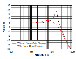
In a difference amplifier circuit, typically used for low side current sensing applications, the (noise gain) = (signal gain + 1).
 Figure 9-6 Noninverting Gain of 3 V/V, 6 V/V
Configurations and Difference Amplifier in Signal Gain of 2 V/V
 Figure 9-7 Small-Signal Frequency Response in Gains of 3V/V (a) and 6V/V (b)
 Figure 9-8 Small-Signal Frequency Response of Difference Amplifier (c) With and
Without Noise Gain Shaping