SBOSAA5C april 2022 – may 2023 OPA2675
PRODUCTION DATA
- 1
- 1 Features
- 2 Applications
- 3 Description
- 4 Revision History
- 5 Device Family Comparison Table
- 6 Pin Configuration and Functions
-
7 Specifications
- 7.1 Absolute Maximum Ratings
- 7.2 ESD Ratings
- 7.3 Recommended Operating Conditions
- 7.4 Thermal Information
- 7.5 Electrical Characteristics: Full Bias and Offline Mode VS = ±6 V
- 7.6 Electrical Characteristics: 75% Bias Mode VS = ±6 V
- 7.7 Electrical Characteristics: 50% Bias Mode VS = ±6 V
- 7.8 Electrical Characteristics: DIfferential Output VS = 12 V
- 7.9 Electrical Characteristics: VS = 5 V
- 7.10 Typical Characteristics: VS = ±6 V, Full Bias
- 7.11 Typical Characteristics: VS = ±6 V Differential, Full Bias
- 7.12 Typical Characteristics: VS = ±6 V, 75% Bias
- 7.13 Typical Characteristics: VS = ±6 V, 50% Bias
- 8 Detailed Description
- 9 Application and Implementation
- 10Device and Documentation Support
- 11Mechanical, Packaging, and Orderable Information
Package Options
Mechanical Data (Package|Pins)
- RGV|16
Thermal pad, mechanical data (Package|Pins)
- RGV|16
Orderable Information
3 Description
The OPA2675 provides the high output current and low distortion required for power-line modem driver and test and measurement applications. The OPA2675 operates on power-supplies ranging from 4.5 V to 13 V and consumes a low 16.5 mA/channel quiescent current to deliver a very high 1000 mA output current. The OPA2675 supports the most demanding power-line modem requirements with an 850 mA specified minimum output current drive (at 25°C).
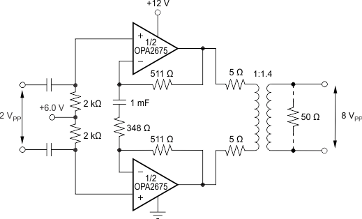
Power-control features are included to minimize system power consumption. Two logic-control lines allow for four quiescent power settings, full power, 75% bias power, 50% bias power, and offline mode with active offline control, to provide high impedance to large signals present at the output pin. The two channels of the OPA2675 can be used independently as individual op amps, or can be configured as a differential-input to differential-output, high-current line driver.
 Single-Supply PLC Line Driver
 50-Ω
Transmission Line Driver