SBOS789C August   2017  – February 2020 OPA2810

PRODUCTION DATA.  

  1. Features
  2. Applications
  3. Description
    1.     Device Images
      1.      Multichannel Sensor Interface
      2.      Harmonic Distortion vs Frequency
  4. Revision History
  5. Device Comparison Table
  6. Pin Configuration and Functions
    1.     Pin Functions
  7. Specifications
    1. 7.1  Absolute Maximum Ratings
    2. 7.2  ESD Ratings
    3. 7.3  Recommended Operating Conditions
    4. 7.4  Thermal Information
    5. 7.5  Electrical Characteristics: 10 V
    6. 7.6  Electrical Characteristics: 24 V
    7. 7.7  Electrical Characteristics: 5 V
    8. 7.8  Typical Characteristics: VS = 10 V
    9. 7.9  Typical Characteristics: VS = 24 V
    10. 7.10 Typical Characteristics: VS = 5 V
    11. 7.11 Typical Characteristics: ±2.375 V to ±12 V Split Supply
  8. Detailed Description
    1. 8.1 Overview
    2. 8.2 Functional Block Diagram
    3. 8.3 Feature Description
      1. 8.3.1 OPA2810 Architecture
      2. 8.3.2 ESD Protection
    4. 8.4 Device Functional Modes
      1. 8.4.1 Split-Supply Operation (±2.375 V to ±13.5 V)
      2. 8.4.2 Single-Supply Operation (4.75 V to 27 V)
  9. Application and Implementation
    1. 9.1 Application Information
      1. 9.1.1 Selection of Feedback Resistors
      2. 9.1.2 Noise Analysis and the Effect of Resistor Elements on Total Noise
    2. 9.2 Typical Applications
      1. 9.2.1 Transimpedance Amplifier
        1. 9.2.1.1 Design Requirements
        2. 9.2.1.2 Detailed Design Procedure
      2. 9.2.2 Multichannel Sensor Interface
  10. 10Power Supply Recommendations
  11. 11Layout
    1. 11.1 Layout Guidelines
      1. 11.1.1 Thermal Considerations
    2. 11.2 Layout Example
  12. 12Device and Documentation Support
    1. 12.1 Documentation Support
      1. 12.1.1 Related Documentation
    2. 12.2 Receiving Notification of Documentation Updates
    3. 12.3 Community Resources
    4. 12.4 Trademarks
    5. 12.5 Electrostatic Discharge Caution
    6. 12.6 Glossary
  13. 13Mechanical, Packaging, and Orderable Information

Package Options

Mechanical Data (Package|Pins)
Thermal pad, mechanical data (Package|Pins)
Orderable Information

Typical Characteristics: ±2.375 V to ±12 V Split Supply

at VO = 2 VPP, RF = 1 kΩ, RL = 1 kΩ and TA ≈ 25°C (unless otherwise noted)
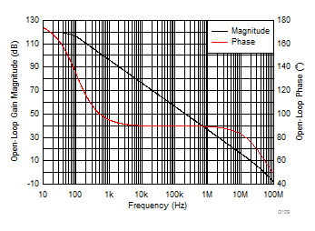
OPA2810 D109_SBOS789_Open_Loop_Gain_Phase1.gif
Simulated with no output load
Figure 44. Open-Loop Gain and Phase vs Frequency
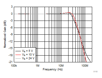
OPA2810 D102_SBOS789_LSBW_Vs_Supply_gain2_All_Supply.gif
See Figure 64, Gain = 2 V/V
Figure 46. Large-Signal Response vs Supply Voltage
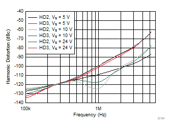
OPA2810 D104_SBOS789_HD_Vs_Freq_Supply_Gain-1.gif
See Figure 65, Gain = –1 V/V
Figure 48. Harmonic Distortion vs Frequency vs Supply Voltage
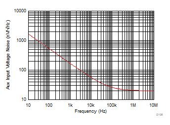
OPA2810 D106_SBOS789_VoltageNoise_Aux.gif
Measured then fit to ideal 1/f model
Figure 50. Auxiliary Input Stage Voltage Noise Density vs Frequency
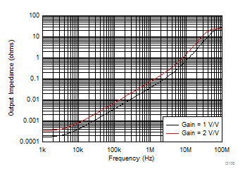
OPA2810 D108_SBOS789_Zout_All_Gains.gif
See Figure 64 (simulation)
Figure 52. Closed-Loop Output Impedance vs Frequency
OPA2810 D111_SBOS789_PSRR_5V_10V.gif
Simulated Curves, VS = 5 V and 10 V
Figure 54. Power Supply Rejection Ratio vs Frequency
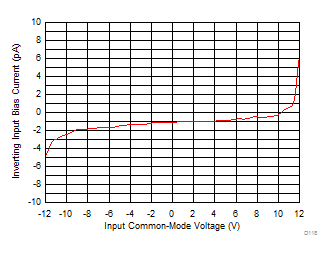
OPA2810 D118_SBOS789_Ibias_vs_Vcm.gif
VS = ±12-V
Figure 56. Input Bias Current vs Input Common-Mode Voltage
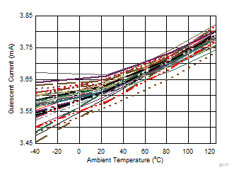
OPA2810 D117_SBOS789_Iq_vs_Temp.gif
70 units, DGK package
Figure 58. Quiescent Current vs Ambient Temperature
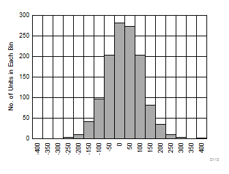
OPA2810 D113_SBOS789_Vos_Distribution.gif
Input offset voltage (µV), 1246 units
Figure 60. Input Offset Voltage Distribution
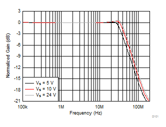
OPA2810 D101_SBOS789_LSBW_Vs_Supply_gain1_All_Supply.gif
See Figure 64, Gain = 1 V/V, RF = 0 Ω
Figure 45. Large-Signal Response vs Supply Voltage
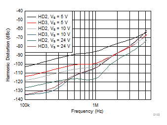
OPA2810 D103_SBOS789_HD_Vs_Freq_Supply.gif
See Figure 64, Gain = 2 V/V
Figure 47. Harmonic Distortion vs Frequency vs Supply Voltage
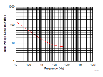
OPA2810 D105_SBOS789_VoltageNoise_JFET.gif
Measured then fit to ideal 1/f model
Figure 49. Input Voltage Noise Density vs Frequency
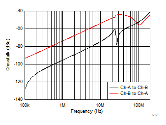
OPA2810 D107_SBOS789_Crosstalk.gif
See Figure 64, Gain = 1 V/V, RF = 0 Ω
Figure 51. Crosstalk vs Frequency
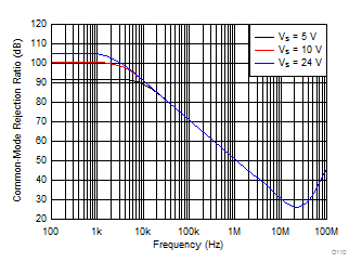
OPA2810 D110_SBOS789_CMRR.gif
Simulated curves
Figure 53. Common-Mode Rejection Ratio vs Frequency
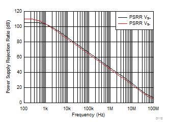
OPA2810 D112_SBOS789_PSRR_24V.gif
Simulated curves, VS = 24 V
Figure 55. Power Supply Rejection Ratio vs Frequency
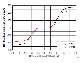
OPA2810 D115_SBOS789_Vindiff_vs_Ibias.gif
Abs (VIN,Diff (max)) = VS when VS < 7 V
Figure 57. Input Bias Current vs Differential Input Voltage
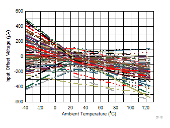
OPA2810 D116_SBOS789_Vos_vs_Temp.gif
70 units, DGK package
Figure 59. Input Offset Voltage vs Ambient Temperature
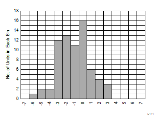
OPA2810 D114_SBOS789_Vos_Drift_DGK_Distribution.gif
Input offset voltage drift (µV/°C), –40°C to +125°C fit, 70 units
Figure 61. Input Offset Voltage Drift Distribution