SBOS973A June   2019  – September 2019 OPA2834

PRODUCTION DATA.  

  1. Features
  2. Applications
  3. Description
    1.     Device Images
      1.      1-kHz FFT Plot (VOUT = 1 VRMS, RL = 100 kΩ, G = 1)
      2.      Low-Side, Current-Shunt Monitoring
  4. Revision History
  5. Device Comparison Table
  6. Pin Configuration and Functions
    1.     Pin Functions
  7. Specifications
    1. 7.1 Absolute Maximum Ratings
    2. 7.2 ESD Ratings
    3. 7.3 Recommended Operating Conditions
    4. 7.4 Thermal Information
    5. 7.5 Electrical Characteristics: 3V to 5V
    6. 7.6 Typical Characteristics: Vs = 5 V
    7. 7.7 Typical Characteristics: VS = 3.0 V
    8. 7.8 Typical Characteristics: ±2.5-V to ±1.5-V Split Supply
  8. Detailed Description
    1. 8.1 Overview
    2. 8.2 Functional Block Diagrams
    3. 8.3 Feature Description
      1. 8.3.1 Input Common-Mode Voltage Range
      2. 8.3.2 Output Voltage Range
      3. 8.3.3 Low-Power Applications and the Effects of Resistor Values on Bandwidth
      4. 8.3.4 Driving Capacitive Loads
    4. 8.4 Device Functional Modes
      1. 8.4.1 Split-Supply Operation (±1.35 V to ±2.7 V)
      2. 8.4.2 Single-Supply Operation (2.7 V to 5.4 V)
  9. Application and Implementation
    1. 9.1 Application Information
      1. 9.1.1 Noninverting Amplifier
      2. 9.1.2 Inverting Amplifier
    2. 9.2 Typical Applications
      1. 9.2.1 Low-Side Current Sensing
        1. 9.2.1.1 Design Requirements
        2. 9.2.1.2 Detailed Design Procedure
      2. 9.2.2 Field Transmitter Sensor Interface
      3. 9.2.3 Ultrasonic Flow Meters
      4. 9.2.4 Microphone Pre-Amplifier
  10. 10Power Supply Recommendations
  11. 11Layout
    1. 11.1 Layout Guidelines
    2. 11.2 Layout Examples
  12. 12Device and Documentation Support
    1. 12.1 Documentation Support
      1. 12.1.1 Related Documentation
    2. 12.2 Receiving Notification of Documentation Updates
    3. 12.3 Community Resources
    4. 12.4 Trademarks
    5. 12.5 Electrostatic Discharge Caution
    6. 12.6 Glossary
  13. 13Mechanical, Packaging, and Orderable Information

Package Options

Mechanical Data (Package|Pins)
Thermal pad, mechanical data (Package|Pins)
Orderable Information

Typical Characteristics: ±2.5-V to ±1.5-V Split Supply

with PD = VCC and TA ≈ 25°C , gain mentioned in V/V (unless otherwise noted)
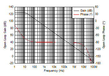
OPA2834 D313_aol_phase.gif
Figure 29. Open-Loop Gain and Phase vs Frequency
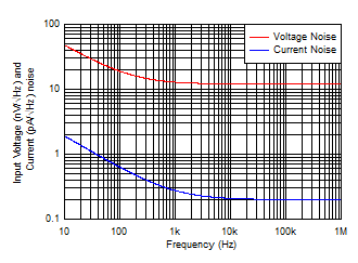
OPA2834 D100_Noise_Frequency.gif
Measured then fit to ideal 1/f model
Figure 31. Input Noise Density vs Frequency
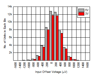
OPA2834 D151_offsethistogram_new.gif
54000 units at each supply voltage
Figure 33. Input Offset Voltage Distribution
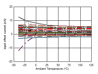
OPA2834 D154_input_offset_current.gif
32 units at 5-V and 3-V supply
Figure 35. Input Offset Current vs Ambient Temperature
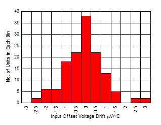
OPA2834 D142_offsetDrift_histogram.gif
136 units, –40°C to +125°C
Figure 37. Input Offset Voltage Drift Distribution
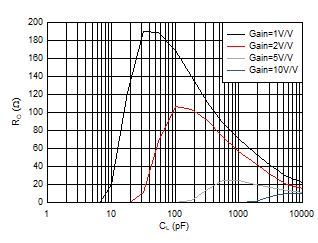
OPA2834 D301_Riso_vs_Cload.gif
See Figure 49,
Recommended value of RO for targeting 30° phase margin
Figure 39. Output Resistor (RO) vs CL
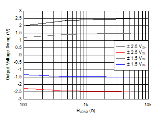
OPA2834 D316_Outputswingvsresisotor.gif
Figure 41. Output Voltage Swing vs Load Resistor
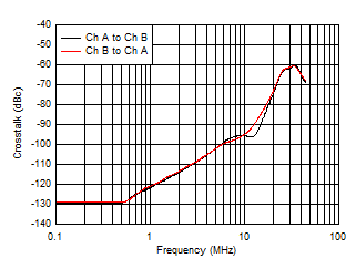
OPA2834 D107_Crosstalk.gif
Figure 43. Crosstalk vs Frequency
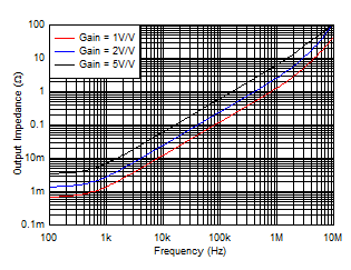
OPA2834 D314_zout_frequency.gif
Figure 30. Closed-Loop Output Impedance vs Frequency
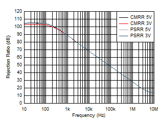
OPA2834 D315_CMRR_PSRR_FREQ.gif
Figure 32. CMRR and PSRR vs Frequency
OPA2834 D141_offset_vs_Temperature.gif
32 units at 5-V and 3-V supply, Input offset voltage calibrated to 0V at 25°C
Figure 34. Input Offset Voltage vs Ambient Temperature
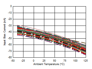
OPA2834 D153_biascurrentvstemp.gif
32 units at 5-V and 3-V supply
Figure 36. Input Bias Current vs Ambient Temperature
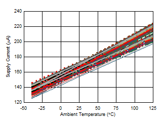
OPA2834 D150_quiescent_current.gif
32 units at 5-V and 3-V supply
Figure 38. Supply Current vs Ambient Temperature
OPA2834 D302_recommededROvsCL_Frequencyresponse.gif
See Figure 49
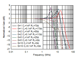
Figure 40. Small-Signal Frequency Response vs CL
With Recommended RO
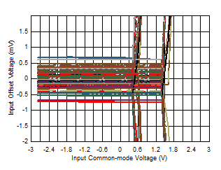
OPA2834 D317_Vos_Vcm.gif
32 units at 5-V and 3-V supplies
Figure 42. Input Offset Voltage vs Input Common-Mode Voltage
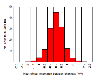
OPA2834 D300_OffsetMismatch_histogram.gif
Figure 44. Input Offset Mismatch (Between Channel A and Channel B) Distribution