SBOS982J june 2020 – june 2023 OPA2863 , OPA4863 , OPA863
PRODUCTION DATA
- 1
- 1 Features
- 2 Applications
- 3 Description
- 4 Revision History
- 5 Device Comparison Table
- 6 Pin Configuration and Functions
-
7 Specifications
- 7.1 Absolute Maximum Ratings
- 7.2 ESD Ratings
- 7.3 Recommended Operating Conditions
- 7.4 Thermal Information: OPA863
- 7.5 Thermal Information: OPA2863
- 7.6 Thermal Information: OPA4863
- 7.7 Electrical Characteristics: VS = 10 V
- 7.8 Electrical Characteristics: VS = 3 V
- 7.9 Typical Characteristics: VS = 10 V
- 7.10 Typical Characteristics: VS = 3 V
- 7.11 Typical Characteristics: VS = 3 V to 10 V
- 8 Detailed Description
- 9 Application and Implementation
- 10Device and Documentation Support
- 11Mechanical, Packaging, and Orderable Information
Package Options
Mechanical Data (Package|Pins)
Thermal pad, mechanical data (Package|Pins)
Orderable Information
9.2.2 Front-End Gain and Filtering
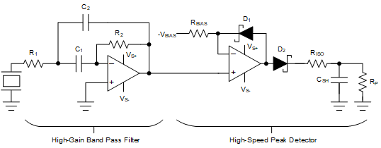
 Figure 9-3 High-Gain Narrow Bandpass
Filter and Peak Detector Circuit
Figure 9-3 High-Gain Narrow Bandpass
Filter and Peak Detector CircuitUltrasonic signaling is used for proximity and obstacle detection, level sensing, sonars, and so forth. Such signal chains detect the amplitude of received ultrasonic signal at a particular center frequency. Figure 9-3 shows a high-gain narrow bandpass filter and peak detector circuit using any of the OPAx863 devices. The signal at the frequency of interest is filtered out, gained, and peak detected to report the amplitude at the output of this circuit. The phase information is lost in this circuit. The OPAx863 devices are used with the 50-MHz GBW to add a single-stage gain and filtering, and the peak detection capability is easily made with the RRIO capability of these amplifiers.