SBOS969F October 2019 – January 2022 OPA2991 , OPA4991 , OPA991
PRODMIX
- 1 Features
- 2 Applications
- 3 Description
- 4 Revision History
- 5 Pin Configuration and Functions
- 6 Specifications
-
7 Detailed Description
- 7.1 Overview
- 7.2 Functional Block Diagram
- 7.3
Feature Description
- 7.3.1 Input Protection Circuitry
- 7.3.2 EMI Rejection
- 7.3.3 Thermal Protection
- 22
- 7.3.4 Capacitive Load and Stability
- 7.3.5 Common-Mode Voltage Range
- 7.3.6 Phase Reversal Protection
- 7.3.7 Electrical Overstress
- 7.3.8 Overload Recovery
- 7.3.9 Typical Specifications and Distributions
- 7.3.10 Packages With an Exposed Thermal Pad
- 7.3.11 Shutdown
- 7.4 Device Functional Modes
- 8 Application and Implementation
- 9 Power Supply Recommendations
- 10Layout
- 11Device and Documentation Support
- 12Mechanical, Packaging, and Orderable Information
8.2.1.2 Detailed Design Procedure
The transfer function of the circuit in Figure 8-1 is given in Equation 1:

The load current (ILOAD) produces a voltage drop across the shunt resistor (RSHUNT). The load current is set from 0 A to 1 A. To keep the shunt voltage below 100 mV at maximum load current, the largest shunt resistor is defined using Equation 2:
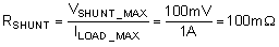
Using Equation 2, RSHUNT is calculated to be 100 mΩ. The voltage drop produced by ILOAD and RSHUNT is amplified by the OPA991 to produce an output voltage of 0 V to 4.9 V. The gain needed by the OPA991 to produce the necessary output voltage is calculated using Equation 3:
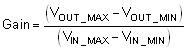
Using Equation 3, the required gain is calculated to be 49 V/V, which is set with resistors RF and RG. Equation 4 is used to size the resistors, RF and RG, to set the gain of the OPA991 to 49 V/V.

Choosing RF as 360 kΩ, RG is calculated to be 7.5 kΩ. RF and RG were chosen as 360 kΩ and 7.5 kΩ because they are standard value resistors that create a 49:1 ratio. Other resistors that create a 49:1 ratio can also be used. Figure 8-2 shows the measured transfer function of the circuit shown in Figure 8-1.