SBOS512E March 2010 – November 2020 OPA2365-Q1 , OPA365-Q1
PRODUCTION DATA
- 1 Features
- 2 Applications
- 3 Description
- 4 Revision History
- 5 Pin Configuration and Functions
- 6 Specifications
- 7 Detailed Description
- 8 Application and Implementation
- 9 Power Supply Recommendations
- 10Layout
- 11Device and Documentation Support
- 12Mechanical, Packaging, and Orderable Information
Package Options
Mechanical Data (Package|Pins)
- DBV|5
Thermal pad, mechanical data (Package|Pins)
Orderable Information
8.2.2.2 Detailed Design Procedure
Some applications need bandpass filter–that is, radar or audio signal precessing. The cross over frequencies and flat gain can be adjusted by changing the resistors and capacitors value according to applications.
The circuit is designed for 5-V supply and 20-mV input signal. With a flat gain of 100 dB or 40 dB, the peak output signal is 2 V. The reference signal is at half way of 5 V, which is 2.5 V.
Equation 1. 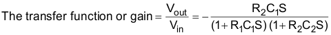
Equation 2. 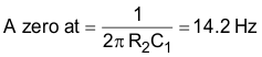
Equation 3. 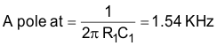
Equation 4. 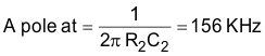
Equation 5. Flat Gain of 100 or 40 dB between 1.54 kHz and 156 kHz
Equation 6. 20 db/decade below 1.54 KHz
Equation 7. –20 dB/decade above 156 kHz
Equation 8. Bandpass between 1.54 kHz and 156 kHz