SBOS512E March 2010 – November 2020 OPA2365-Q1 , OPA365-Q1
PRODUCTION DATA
- 1 Features
- 2 Applications
- 3 Description
- 4 Revision History
- 5 Pin Configuration and Functions
- 6 Specifications
- 7 Detailed Description
- 8 Application and Implementation
- 9 Power Supply Recommendations
- 10Layout
- 11Device and Documentation Support
- 12Mechanical, Packaging, and Orderable Information
Package Options
Mechanical Data (Package|Pins)
- DBV|5
Thermal pad, mechanical data (Package|Pins)
Orderable Information
8.1.2 Achieving an Output Level of Zero Volts (0 V)
Certain single-supply applications require the operational amplifier output to swing from 0 V to a positive full-scale voltage and have high accuracy. An example is an operational amplifier employed to drive a single-supply ADC having an input range from 0 V to 5 V. Rail-to-rail output amplifiers with very light output loading may achieve an output level within millivolts of 0 V (or +VS at the high end), but not 0 V. Furthermore, the deviation from 0 V only becomes greater as the load current required increases. This increased deviation is a result of limitations of the CMOS output stage.
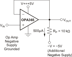
When a pulldown resistor is connected from the amplifier output to a negative voltage source, the OPA365-Q1 can achieve an output level of 0 V, and even a few millivolts below 0 V. Below this limit, nonlinearity and limiting conditions become evident. Figure 8-2 illustrates a circuit using this technique.
 Figure 8-2 Swing-to-Ground
A pulldown current of approximately 500 µA is required when OPA365-Q1 is connected as a unity-gain buffer. A practical termination voltage (VNEG) is −5 V, but other convenient negative voltages also may be used. The pulldown resistor RL is calculated from RL = [(VO −VNEG)/(500 µA)]. Using a minimum output voltage (VO) of 0 V, RL = [0 V−(−5V)]/(500 µA)] = 10 kΩ. Keep in mind that lower termination voltages result in smaller pulldown resistors that load the output during positive output voltage excursions.
This technique does not work with all operational amplifier, and should only be applied to operational amplifiers, such as the OPA365-Q1, that have been specifically designed to operate in this manner. Also, operating the OPA365-Q1 output at 0 V changes the output stage operating conditions, resulting in somewhat lower open-loop gain and bandwidth. Keep these precautions in mind when driving a capacitive load because these conditions can affect circuit transient response and stability.