SBOS777D November 2016 – July 2020 OPA2388 , OPA388 , OPA4388
PRODUCTION DATA
- 1 Features
- 2 Applications
- 3 Description
- 4 Revision History
- 5 Pin Configuration and Functions
- 6 Specifications
- 7 Detailed Description
- 8 Application and Implementation
- 9 Power Supply Recommendations
- 10Layout
- 11Device and Documentation Support
- 12Mechanical, Packaging, and Orderable Information
Package Options
Mechanical Data (Package|Pins)
Thermal pad, mechanical data (Package|Pins)
- DGK|8
Orderable Information
7.3.2 Input Voltage and Zero-Crossover Functionality
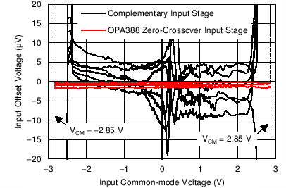
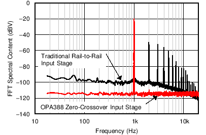
The OPAx388 input common-mode voltage range extends 0.1 V beyond the supply rails. This amplifier family is designed to cover the full range without the troublesome transition region found in some other rail-to-rail amplifiers. Operating a complementary rail-to-rail input amplifier with signals traversing the transition region results in unwanted non-linear behavior and polluted spectral content. Figure 7-1 and Figure 7-2 contrast the performance of a traditional complementary rail-to-rail input stage amplifier with the performance of the zero-crossover OPA388. Significant harmonic content and distortion is generated during the differential pair transition (such a transition does not exist in the OPA388). Crossover distortion is eliminated through the use of a single differential pair coupled with an internal low-noise charge pump. The OPAx388 maintains noise, bandwidth, and offset performance throughout the input common-mode range, thus reducing printed circuit board (PCB) and bill of materials (BOM) complexity through the reduction of power-supply rails.
 Figure 7-1 Input
Crossover Distortion Nonlinearity
 Figure 7-2 Input
Crossover Distortion Spectral Content
Figure 7-2 Input
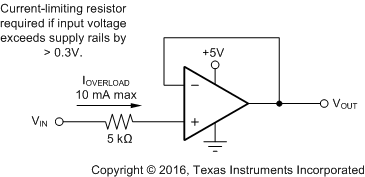
Crossover Distortion Spectral ContentTypically, input bias current is approximately ±30 pA. Input voltages exceeding the power supplies, however, can cause excessive current to flow into or out of the input pins. Momentary voltages greater than the power supply can be tolerated if the input current is limited to 10 mA. This limitation is easily accomplished with an input resistor, as shown in Figure 7-3.
 Figure 7-3 Input
Current Protection