SBOSA65 July   2021 OPA396

PRODUCTION DATA  

  1. Features
  2. Applications
  3. Description
  4. Revision History
  5. Pin Configuration and Functions
  6. Specifications
    1. 6.1 Absolute Maximum Ratings
    2. 6.2 ESD Ratings
    3. 6.3 Recommended Operating Conditions
    4. 6.4 Thermal Information
    5. 6.5 Electrical Characteristics
    6. 6.6 Typical Characteristics
  7. Detailed Description
    1. 7.1 Overview
    2. 7.2 Functional Block Diagram
    3. 7.3 Feature Description
      1. 7.3.1 Low Input Bias Current
      2. 7.3.2 Input Differential Voltage
      3. 7.3.3 Capacitive Load Drive
      4. 7.3.4 EMI Rejection
    4. 7.4 Device Functional Modes
  8. Application and Implementation
    1. 8.1 Application Information
    2. 8.2 Typical Applications
      1. 8.2.1 Three-Terminal CO Gas Sensor
        1. 8.2.1.1 Design Requirements
        2. 8.2.1.2 Detailed Design Procedure
        3. 8.2.1.3 Application Curve
      2. 8.2.2 4-mA to 20-mA Loop Design
        1. 8.2.2.1 Design Requirements
        2. 8.2.2.2 Application Curve
  9. Power Supply Recommendations
  10. 10Layout
    1. 10.1 Layout Guidelines
    2. 10.2 Layout Example
  11. 11Device and Documentation Support
    1. 11.1 Device Support
      1. 11.1.1 Development Support
        1. 11.1.1.1 TINA-TI™ Simulation Software (Free Download)
    2. 11.2 Documentation Support
      1. 11.2.1 Related Documentation
    3. 11.3 Receiving Notification of Documentation Updates
    4. 11.4 Support Resources
    5. 11.5 Trademarks
    6. 11.6 Electrostatic Discharge Caution
    7. 11.7 Glossary
  12. 12Mechanical, Packaging, and Orderable Information

Package Options

Mechanical Data (Package|Pins)
Thermal pad, mechanical data (Package|Pins)
Orderable Information

Input Differential Voltage

The OPA396 does not have any diodes connected between the input nodes, allowing for input voltages anywhere between the supply voltage. The input structure can be seen in Figure 7-1. Although the device can tolerate any differential input voltage that does not exceed the supply voltage, do not operate continuously at differential input voltages greater than 0.5 V.
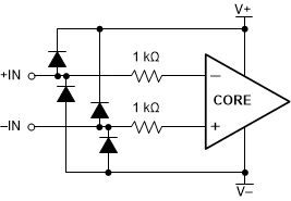
GUID-20201118-CA0I-MMBT-WDV3-RKHNGGMQQRZJ-low.gif Figure 7-1 Equivalent Input Circuit