SBOS701D December 2015 – August 2021 OPA191 , OPA2191 , OPA4191
PRODUCTION DATA
- 1 Features
- 2 Applications
- 3 Description
- 4 Revision History
- 5 Pin Configuration and Functions
-
6 Specifications
- 6.1 Absolute Maximum Ratings
- 6.2 ESD Ratings
- 6.3 Recommended Operating Conditions
- 6.4 Thermal Information: OPA191
- 6.5 Thermal Information: OPA2191
- 6.6 Thermal Information: OPA4191
- 6.7 Electrical Characteristics: VS = ±4 V to ±18 V (VS = 8 V to 36 V)
- 6.8 Electrical Characteristics: VS = ±2.25 V to ±4 V (VS = 4.5 V to 8 V)
- 6.9 Typical Characteristics
- 7 Parameter Measurement Information
- 8 Detailed Description
- 9 Application and Implementation
- 10Power Supply Recommendations
- 11Layout
- 12Device and Documentation Support
- 13Mechanical, Packaging, and Orderable Information
Package Options
Mechanical Data (Package|Pins)
Thermal pad, mechanical data (Package|Pins)
- RUM|16
Orderable Information
8.3.3 Phase Reversal Protection
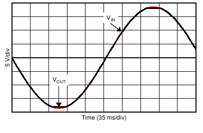
The OPAx191 family has internal phase-reversal protection. Many op amps exhibit phase reversal when the input is driven beyond the linear common-mode range. This condition is most often encountered in noninverting circuits when the input is driven beyond the specified common-mode voltage range, causing the output to reverse into the opposite rail. The OPAx191 is a rail-to-rail input op amp, and therefore the common-mode range can extend up to the rails. Input signals beyond the rails do not cause phase reversal; instead, the output limits into the appropriate rail. This performance is shown in Figure 8-4.
 Figure 8-4 No Phase Reversal