SBOS703F April 2014 – October 2016 OPA2316 , OPA316 , OPA4316
PRODUCTION DATA.
- 1 Features
- 2 Applications
- 3 Description
- 4 Revision History
- 5 Pin Configuration and Functions
- 6 Specifications
- 7 Detailed Description
- 8 Application and Implementation
- 9 Power Supply Recommendations
- 10Layout
- 11Device and Documentation Support
- 12Mechanical, Packaging, and Orderable Information
- 11Mechanical, Packaging, and Orderable Information
Package Options
Mechanical Data (Package|Pins)
Thermal pad, mechanical data (Package|Pins)
Orderable Information
5 Pin Configuration and Functions
DCK Package
5-Pin SC70
Top View
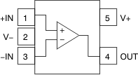
DBV Package
5-Pin SOT-23
Top View
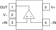
8-Pin DFN
Top View
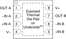
NOINDENT:
Pitch: 0.5 mm.NOINDENT:
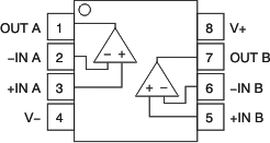
Connect thermal pad to V–. Pad size: 2.00 mm × 1.20 mm.D, DGK Packages
8-Pin MSOP, SO
Top View
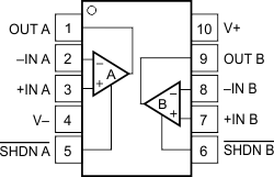
DGS Package
10-Pin MSOP
Top View
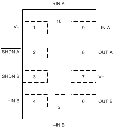
RUG Package
10-Pin QFN
Top View
Pin Functions
| PIN | DESCRIPTION | |||||||
|---|---|---|---|---|---|---|---|---|
| NAME | OPA316 | OPA2316 | OPA2316S | OPA4316 | ||||
| DBV | DCK | D, DGK, DRG | DGS | RUG | PW | D | ||
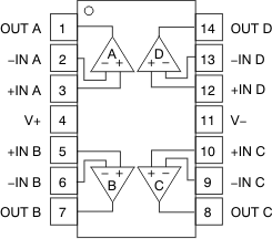
| +IN | 3 | 1 | — | — | — | — | — | Noninverting input |
| +IN A | — | — | 3 | 3 | 10 | 3 | 3 | Noninverting input |
| +IN B | — | — | 5 | 7 | 4 | 5 | 5 | Noninverting input |
| +IN C | — | — | — | — | — | 10 | 10 | Noninverting input |
| +IN D | — | — | — | — | — | 12 | 12 | Noninverting input |
| –IN | 4 | 3 | — | — | — | — | — | Inverting input |
| –IN A | — | — | 2 | 2 | 9 | 2 | 2 | Inverting input |
| –IN B | — | — | 6 | 8 | 5 | 6 | 6 | Inverting input |
| –IN C | — | — | — | — | — | 9 | 9 | Inverting input |
| –IN D | — | — | — | — | — | 13 | 13 | Inverting input |
| OUT | 1 | 4 | — | — | — | — | — | Output |
| OUT A | — | — | 1 | 1 | 8 | 1 | 1 | Output |
| OUT B | — | — | 7 | 9 | 6 | 7 | 7 | Output |
| OUT C | — | — | — | — | — | 8 | 8 | Output |
| OUT D | — | — | — | — | — | 14 | 14 | Output |
| SHDN A | — | — | — | 5 | 2 | — | — | Shutdown (logic low), enable (logic high) |
| SHDN B | — | — | — | 6 | 3 | — | — | Shutdown (logic low), enable (logic high) |
| V+ | 5 | 5 | 8 | 10 | 7 | 4 | 4 | Positive supply |
| V– | 2 | 2 | 4 | 4 | 1 | 11 | 11 | Negative supply or ground (for single-supply operation) |
