SBOS982J june 2020 – june 2023 OPA2863 , OPA4863 , OPA863
PRODUCTION DATA
- 1
- 1 Features
- 2 Applications
- 3 Description
- 4 Revision History
- 5 Device Comparison Table
- 6 Pin Configuration and Functions
-
7 Specifications
- 7.1 Absolute Maximum Ratings
- 7.2 ESD Ratings
- 7.3 Recommended Operating Conditions
- 7.4 Thermal Information: OPA863
- 7.5 Thermal Information: OPA2863
- 7.6 Thermal Information: OPA4863
- 7.7 Electrical Characteristics: VS = 10 V
- 7.8 Electrical Characteristics: VS = 3 V
- 7.9 Typical Characteristics: VS = 10 V
- 7.10 Typical Characteristics: VS = 3 V
- 7.11 Typical Characteristics: VS = 3 V to 10 V
- 8 Detailed Description
- 9 Application and Implementation
- 10Device and Documentation Support
- 11Mechanical, Packaging, and Orderable Information
Package Options
Mechanical Data (Package|Pins)
- PW|14
Thermal pad, mechanical data (Package|Pins)
- PW|14
Orderable Information
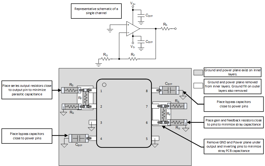
9.4.2 Layout Example
 Figure 9-7 Layout
Recommendation for Dual-Channel DGK Package