SBOS969F October 2019 – January 2022 OPA2991 , OPA4991 , OPA991
PRODMIX
- 1 Features
- 2 Applications
- 3 Description
- 4 Revision History
- 5 Pin Configuration and Functions
- 6 Specifications
-
7 Detailed Description
- 7.1 Overview
- 7.2 Functional Block Diagram
- 7.3
Feature Description
- 7.3.1 Input Protection Circuitry
- 7.3.2 EMI Rejection
- 7.3.3 Thermal Protection
- 22
- 7.3.4 Capacitive Load and Stability
- 7.3.5 Common-Mode Voltage Range
- 7.3.6 Phase Reversal Protection
- 7.3.7 Electrical Overstress
- 7.3.8 Overload Recovery
- 7.3.9 Typical Specifications and Distributions
- 7.3.10 Packages With an Exposed Thermal Pad
- 7.3.11 Shutdown
- 7.4 Device Functional Modes
- 8 Application and Implementation
- 9 Power Supply Recommendations
- 10Layout
- 11Device and Documentation Support
- 12Mechanical, Packaging, and Orderable Information
Package Options
Mechanical Data (Package|Pins)
Thermal pad, mechanical data (Package|Pins)
- PW|14
Orderable Information
7.3.4 Capacitive Load and Stability
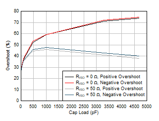
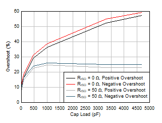
The OPAx991 features a resistive output stage capable of driving moderate capacitive loads, and by leveraging an isolation resistor, the device can easily be configured to drive large capacitive loads. Increasing the gain enhances the ability of the amplifier to drive greater capacitive loads; see Figure 7-5 and Figure 7-6. The particular op amp circuit configuration, layout, gain, and output loading are some of the factors to consider when establishing whether an amplifier will be stable in operation.
 Figure 7-5 Small-Signal Overshoot vs Capacitive Load (10-mV Output Step, G = 1)
 Figure 7-6 Small-Signal Overshoot vs Capacitive Load (10-mV Output Step, G = –1)
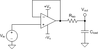
For additional drive capability in unity-gain configurations, improve capacitive load drive by inserting a small resistor, RISO, in series with the output, as shown in Figure 7-7. This resistor significantly reduces ringing and maintains DC performance for purely capacitive loads. However, if a resistive load is in parallel with the capacitive load, then a voltage divider is created, thus introducing a gain error at the output and slightly reducing the output swing. The error introduced is proportional to the ratio RISO / RL, and is generally negligible at low output levels. A high capacitive load drive makes the OPAx991 well suited for applications such as reference buffers, MOSFET gate drives, and cable-shield drives. The circuit shown in Figure 7-7 uses an isolation resistor, RISO, to stabilize the output of an op amp. RISO modifies the open-loop gain of the system for increased phase margin.
 Figure 7-7 Extending Capacitive Load Drive With the OPA991