SBOS940A May 2019 – March 2020 OPA818
PRODUCTION DATA.
- 1 Features
- 2 Applications
- 3 Description
- 4 Revision History
- 5 Device Comparison Table
- 6 Pin Configuration and Functions
- 7 Specifications
- 8 Detailed Description
- 9 Application and Implementation
- 10Power Supply Recommendations
- 11Layout
- 12Device and Documentation Support
- 13Mechanical, Packaging, and Orderable Information
Package Options
Mechanical Data (Package|Pins)
- DRG|8
Thermal pad, mechanical data (Package|Pins)
- DRG|8
Orderable Information
8.3.3 Decompensated Architecture With Wide Gain-Bandwidth Product
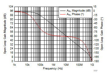
Figure 47 shows the open-loop gain and phase response of the OPA818. The GBWP of an op amp is measured in the 20 dB/decade constant slope region of the AOL magnitude plot. The open-loop gain of 60 dB for the OPA818 is along this 20 dB/decade slope and the corresponding frequency intercept is at 2.7 MHz. Converting 60 dB to linear units (1000 V/V) and multiplying it with the 2.7 MHz frequency intercept gives the GBWP of OPA818 as 2.7 GHz. As can be inferred from the AOL Bode plot, the second pole in the AOL response occurs before AOL magnitude drops below 0 dB (1 V/V). This results in phase change of more than 180° at 0 dB AOL indicating that the amplifier will not be stable in a gain of 1 V/V. Amplifiers like OPA818 that are not unity-gain stable are referred to as decompensated amplifiers. The decompensated architecture typically allows for higher GBWP, higher slew rate, and lower noise compared to a unity-gain stable amplifier with equivalent quiescent current. The additional advantage of the decompensated amplifier is better distortion performance at higher frequencies in high gain applications for comparable quiescent current to a unity-gain stable amplifier.
OPA818 is stable in noise gain of 7 V/V (16.9 dB) or higher in conventional gain circuits as shown in Figure 43 and Figure 44. It has 790 MHz of SSBW in this gain configuration with approximately 50° phase margin.
The high GBWP and low voltage and current noise of OPA818 make it a very suitable amplifier for wideband moderate to high transimpedance gain applications. Transimpedance gains of 50 kΩ or higher benefit from the low current noise JFET input. In a typical transimpedance (TIA) circuit as shown in Figure 50, unity-gain stable amplifier is not a requirement. At low frequencies, the noise gain of TIA is 0 dB (1 V/V) and at high frequencies the noise gain is set by the ratio of the total input capacitance (CTOT) and the feedback capacitance (CF). To maximize TIA closed-loop bandwidth, the feedback capacitance is generally smaller than the total input capacitance. This results in the ratio of total input capacitance to the feedback capacitance to be greater than 1, which is ultimately the noise gain of the TIA at higher frequencies. The blog series, What you need to know about transimpedance amplifiers – part 1 and What you need to know about transimpedance amplifiers – part 2 describe TIA compensation techniques in greater detail.

| RL = 100 Ω | Simulation |

| RL = 100 Ω | Simulation |