SBOS940A May 2019 – March 2020 OPA818
PRODUCTION DATA.
- 1 Features
- 2 Applications
- 3 Description
- 4 Revision History
- 5 Device Comparison Table
- 6 Pin Configuration and Functions
- 7 Specifications
- 8 Detailed Description
- 9 Application and Implementation
- 10Power Supply Recommendations
- 11Layout
- 12Device and Documentation Support
- 13Mechanical, Packaging, and Orderable Information
Package Options
Mechanical Data (Package|Pins)
- DRG|8
Thermal pad, mechanical data (Package|Pins)
- DRG|8
Orderable Information
8.3.1 Input and ESD Protection
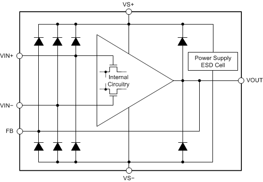
The OPA818 is built using a very high speed complementary bipolar process. The internal junction breakdown voltages are relatively low for these very small geometry devices. These breakdowns are reflected in the Absolute Maximum Ratings table. All device pins are protected with internal ESD protection diodes to the power supplies as shown in Figure 45.
These diodes provide moderate protection to input overdrive voltages beyond the supplies as well. The protection diodes can typically support 10-mA continuous current. Where higher currents are possible (for example, in systems with ±12-V supply parts driving into the OPA818), current limiting series resistors should be added in series with the two inputs to limit the current. Keep these resistor values as low as possible because high values degrade both noise performance and frequency response. There are no back-to-back ESD diodes between VIN+ and VIN–. As a result, the differential input voltage between VIN+ and VIN– is entirely absorbed by the VGS of the input JFET differential pair and must not exceed the voltage ratings shown in Absolute Maximum Ratings table.
 Figure 45. Internal ESD Protection