SBOS940A May   2019  – March 2020 OPA818

PRODUCTION DATA.  

  1. Features
  2. Applications
    1.     High-Speed Optical Front-End
  3. Description
    1.     Photodiode Capacitance vs 3-dB Bandwidth
  4. Revision History
  5. Device Comparison Table
  6. Pin Configuration and Functions
    1.     Pin Functions
  7. Specifications
    1. 7.1 Absolute Maximum Ratings
    2. 7.2 ESD Ratings
    3. 7.3 Recommended Operating Conditions
    4. 7.4 Thermal Information
    5. 7.5 Electrical Characteristics: VS = ±5 V
    6. 7.6 Typical Characteristics: VS = ±5 V
    7. 7.7 Typical Characteristics: VS = 6 V
  8. Detailed Description
    1. 8.1 Overview
    2. 8.2 Functional Block Diagram
    3. 8.3 Feature Description
      1. 8.3.1 Input and ESD Protection
      2. 8.3.2 Feedback Pin
      3. 8.3.3 Decompensated Architecture With Wide Gain-Bandwidth Product
      4. 8.3.4 Low Input Capacitance
    4. 8.4 Device Functional Modes
      1. 8.4.1 Split-Supply Operation (+4/–2 V to ±6.5 V)
      2. 8.4.2 Single-Supply Operation (6 V to 13 V)
  9. Application and Implementation
    1. 9.1 Application Information
      1. 9.1.1 Wideband, Non-Inverting Operation
      2. 9.1.2 Wideband, Transimpedance Design Using OPA818
    2. 9.2 Typical Applications
      1. 9.2.1 High Bandwidth, 100-kΩ Gain Transimpedance Design
        1. 9.2.1.1 Design Requirements
        2. 9.2.1.2 Detailed Design Procedure
        3. 9.2.1.3 Application Curves
      2. 9.2.2 Non-Inverting Gain of 2 V/V
  10. 10Power Supply Recommendations
  11. 11Layout
    1. 11.1 Layout Guidelines
      1. 11.1.1 Thermal Considerations
    2. 11.2 Layout Example
  12. 12Device and Documentation Support
    1. 12.1 Device Support
      1. 12.1.1 Development Support
    2. 12.2 Documentation Support
      1. 12.2.1 Related Documentation
    3. 12.3 Receiving Notification of Documentation Updates
    4. 12.4 Community Resources
    5. 12.5 Trademarks
    6. 12.6 Electrostatic Discharge Caution
    7. 12.7 Glossary
  13. 13Mechanical, Packaging, and Orderable Information

Package Options

Mechanical Data (Package|Pins)
Thermal pad, mechanical data (Package|Pins)
Orderable Information

Pin Configuration and Functions

DRG Package
8-Pin WSON With Thermal Pad
Top View
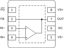
OPA818 SBOS940_OPA818_Pinout-DRG.gif
NC - no internal connection

Pin Functions

PIN TYPE DESCRIPTION
NAME WSON
FB 2 Output Feedback resistor connection (optional)
IN– 3 Input Inverting input
IN+ 4 Input Non-inverting input
NC 6 No connect (no internal connection to die)
OUT 7 Output Output of amplifier
PD 1 Input Power down (low = enable, high = disable); internal 1-MΩ pull-up allows floating this pin
VS– 5 Power Negative power supply
VS+ 8 Power Positive power supply
Thermal pad Electrically isolated from the die substrate but ESD diodes down-bonded to the thermal pad. Recommended connection to a heat spreading plane, typically GND.