SBOS940A May   2019  – March 2020 OPA818

PRODUCTION DATA.  

  1. Features
  2. Applications
    1.     High-Speed Optical Front-End
  3. Description
    1.     Photodiode Capacitance vs 3-dB Bandwidth
  4. Revision History
  5. Device Comparison Table
  6. Pin Configuration and Functions
    1.     Pin Functions
  7. Specifications
    1. 7.1 Absolute Maximum Ratings
    2. 7.2 ESD Ratings
    3. 7.3 Recommended Operating Conditions
    4. 7.4 Thermal Information
    5. 7.5 Electrical Characteristics: VS = ±5 V
    6. 7.6 Typical Characteristics: VS = ±5 V
    7. 7.7 Typical Characteristics: VS = 6 V
  8. Detailed Description
    1. 8.1 Overview
    2. 8.2 Functional Block Diagram
    3. 8.3 Feature Description
      1. 8.3.1 Input and ESD Protection
      2. 8.3.2 Feedback Pin
      3. 8.3.3 Decompensated Architecture With Wide Gain-Bandwidth Product
      4. 8.3.4 Low Input Capacitance
    4. 8.4 Device Functional Modes
      1. 8.4.1 Split-Supply Operation (+4/–2 V to ±6.5 V)
      2. 8.4.2 Single-Supply Operation (6 V to 13 V)
  9. Application and Implementation
    1. 9.1 Application Information
      1. 9.1.1 Wideband, Non-Inverting Operation
      2. 9.1.2 Wideband, Transimpedance Design Using OPA818
    2. 9.2 Typical Applications
      1. 9.2.1 High Bandwidth, 100-kΩ Gain Transimpedance Design
        1. 9.2.1.1 Design Requirements
        2. 9.2.1.2 Detailed Design Procedure
        3. 9.2.1.3 Application Curves
      2. 9.2.2 Non-Inverting Gain of 2 V/V
  10. 10Power Supply Recommendations
  11. 11Layout
    1. 11.1 Layout Guidelines
      1. 11.1.1 Thermal Considerations
    2. 11.2 Layout Example
  12. 12Device and Documentation Support
    1. 12.1 Device Support
      1. 12.1.1 Development Support
    2. 12.2 Documentation Support
      1. 12.2.1 Related Documentation
    3. 12.3 Receiving Notification of Documentation Updates
    4. 12.4 Community Resources
    5. 12.5 Trademarks
    6. 12.6 Electrostatic Discharge Caution
    7. 12.7 Glossary
  13. 13Mechanical, Packaging, and Orderable Information

Package Options

Mechanical Data (Package|Pins)
Thermal pad, mechanical data (Package|Pins)
Orderable Information

Typical Characteristics: VS = ±5 V

At TA ≈ 25°C, VS+ = +5 V, VS– = –5 V, closed-loop gain (G) = 7 V/V, VCM = mid-supply, RF = 301 Ω, RL = 100 Ω to mid-supply, small-signal VO = 100 mVPP, large-signal VO = 2 VPP (unless otherwise noted).
OPA818 D001_10V_SSBW.gif
VO = 100 mVPP
Figure 1. Non-Inverting Small-Signal Frequency Response
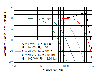
OPA818 D005_LSBW2Vpp10VSupplyGain7,10,20,40,100.gif
VO = 2 VPP
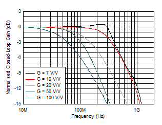
Figure 3. Non-Inverting Large-Signal Frequency Response
OPA818 D007_10V_SSBW_0p1-dB.gif
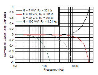
Figure 5. Gain Flatness vs Frequency
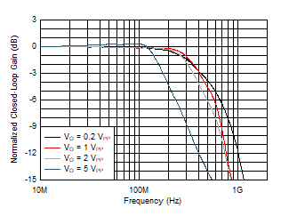
OPA818 D009_LSBW0.2,1,2,5Vpp10VSupplyGain10.gif
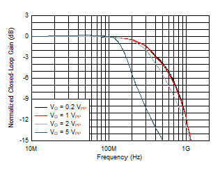
G = 10 V/V
Figure 7. Non-Inverting Frequency Response Over Output Swing
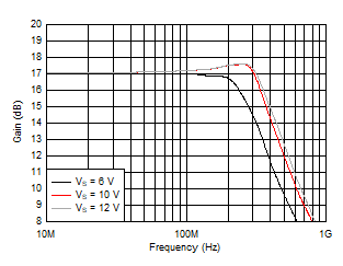
OPA818 D011_SSFR_vs_Vs_100mVpp_G=7_6,10,12Vs.gif
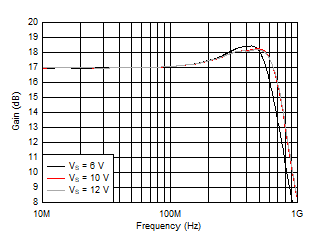
VO = 100 mVPP
Figure 9. Non-Inverting Small-Signal Frequency Response Over Voltage Supply
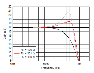
OPA818 D014_SSFR_vs_Rf_100mVpp_10Vs_100-300-500Rf.gif
VO = 100 mVPP
Figure 11. Non-Inverting Small-Signal Frequency Response Over RF
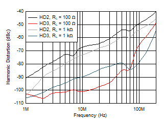
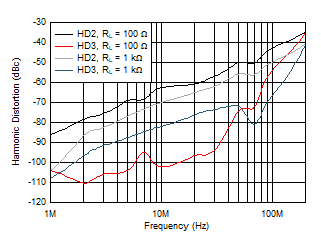
OPA818 D015_HD_vs_Freq_1Vpp_10Vs.gif
VO = 1 VPP
Figure 13. Harmonic Distortion vs Frequency Over RL
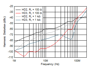
OPA818 D019_HD_vs_Freq_4Vpp_10Vs.gif
VO = 4 VPP
Figure 15. Harmonic Distortion vs Frequency Over RL
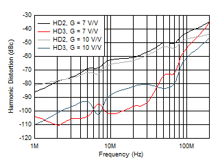
OPA818 D021_HD_vs_Freq_Gain=7,10_2Vpp_10Vs.gif
VO = 2 VPP, Gain = 7 V/V and 10 V/V
Figure 17. Harmonic Distortion vs Frequency Over Gain
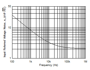
OPA818 D026_10V_Input-noise-density.gif
Figure 19. Voltage Noise Density vs Frequency
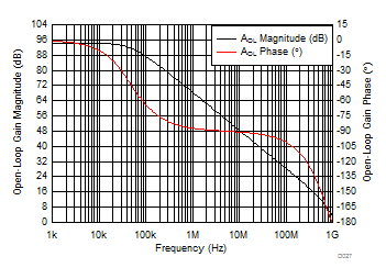
OPA818 D027_10V_Aol_Phase.gif
Simulation
Figure 21. Open-Loop Gain Magnitude and Phase vs Frequency
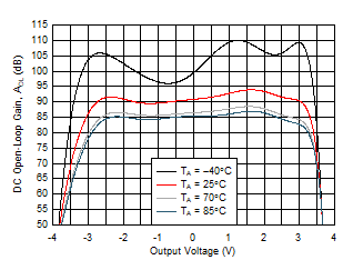
OPA818 D055_10V_Aol_vs_Vo.gif
Figure 23. DC Open-Loop Gain vs Output Voltage
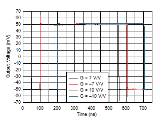
OPA818 D032_SST_100mVpp_Gain=7,-7,10,-10_10Vs.gif
VO = 100-mV step
Figure 25. Small-Signal Pulse Response
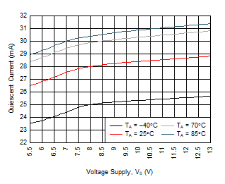
OPA818 D042_10V_Iq_vs_Supply_OverTemp.gif
Figure 27. Quiescent Current vs Voltage Supply Over Temperature
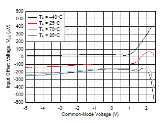
OPA818 D052_10V_Vos_vs_VCM.gif
Figure 29. Input Offset Voltage vs Common-Mode Voltage Over Temperature
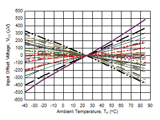
OPA818 D046_10V_Vos_vs_Temperature.gif
35 units, delta from 25°C VOS
Figure 31. Input Offset Voltage vs Temperature
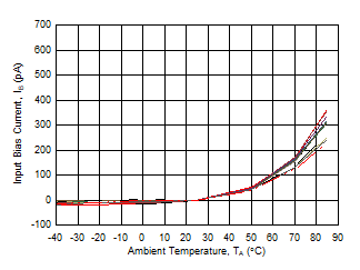
OPA818 D049_10V_Ibp_vs_Temperature.gif
12 units, delta from 25°C IB
Figure 33. Input Bias Current vs Temperature
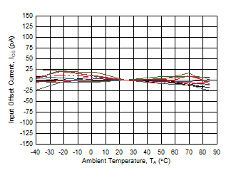
OPA818 D051_10V_Ios_vs_Temperature.gif
12 units, delta from 25°C IOS
Figure 35. Input Offset Current vs Temperature
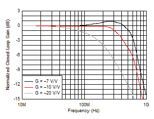
OPA818 D002_SSBW100mVpp10VSupplyGain-7-10-20.gif
VO = 100 mVPP
Figure 2. Inverting Small-Signal Frequency Response
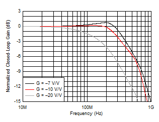
OPA818 D006_LSBW2Vpp10VSupplyGain-7-10-20.gif
VO = 2 VPP
Figure 4. Inverting Large-Signal Frequency Response
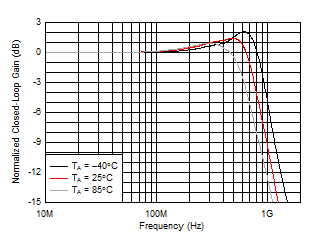
OPA818 D008_SSBW100mVpp10VSupplyGain7_-40,25,85,125C.gif
Figure 6. Non-Inverting Small-Signal Frequency Response Over Temperature
OPA818 D010_LSBW0.2,1,2,5Vpp10VSupplyGain-10.gif
G = –10 V/V
Figure 8. Inverting Frequency Response Over Output Swing
OPA818 D012_LSFR_vs_Vs_2Vpp_G=7_6,10,12Vs.gif
VO = 2 VPP
Figure 10. Non-Inverting Large-Signal Frequency Response Over Voltage Supply
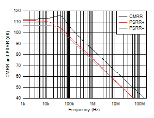
OPA818 D030_10V_CMRR-PSRR_vs_Frequency.gif
Simulation
Figure 12. Common-Mode and Power-Supply Rejection Ratio vs Frequency
OPA818 D017_HD_vs_Freq_2Vpp_10Vs.gif
VO = 2 VPP
Figure 14. Harmonic Distortion vs Frequency Over RL
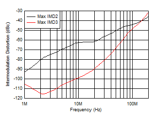
OPA818 D025_IMD_vs_Freq_2Vpp_10Vs.gif
VO = 2 VPP per tone, ±100-kHz tone spacing
Figure 16. Intermodulation Distortion vs Frequency
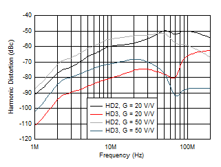
OPA818 D022_HD_vs_Freq_Gain=20,50_2Vpp_10Vs.gif
VO = 2 VPP, Gain = 20 V/V and 50 V/V
Flattening HD at higher frequencies due to bandwidth roll-off
Figure 18. Harmonic Distortion vs Frequency Over Gain
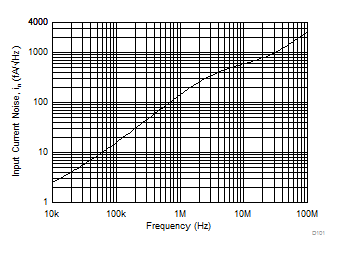
OPA818 D101_10V_Input-current-noise-density.gif
Common-mode noise Simulation
Figure 20. Current Noise Density vs Frequency
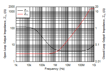
OPA818 D102_10V_Zol-n-Zcl.gif
Simulation
Figure 22. Open-Loop and Closed-Loop Output Impedance vs Frequency
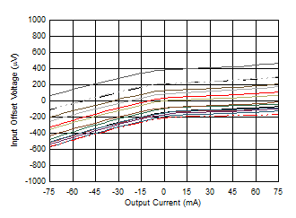
OPA818 D044_10V_Vos_vs_Io.gif
15 units
Figure 24. Input Offset Voltage vs Output Current
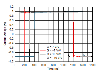
OPA818 D034_LST_2Vpp_Gain=7,-7,10,-10_10Vs.gif
VO = 2-V step
Figure 26. Large-Signal Pulse Response
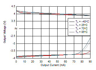
OPA818 D043_10V_Claw_curve.gif
Figure 28. Output Voltage vs Output Current Over Temperature
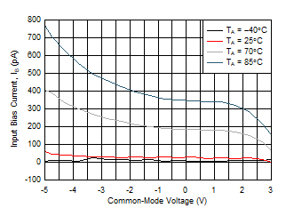
OPA818 D053_10V_Ibp_vs_VCM.gif
Figure 30. Input Bias Current vs Common-Mode Voltage Over Temperature
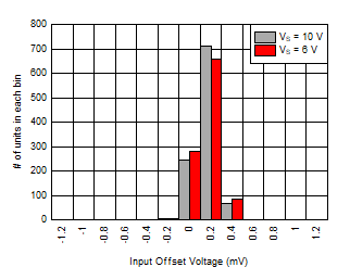
OPA818 D045_10V_6V_Vos-Histo_25C.gif
1000 units at each VS
Figure 32. Input Offset Voltage Histogram
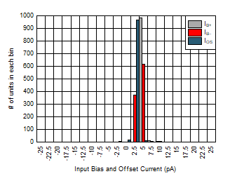
OPA818 D047_10V_Ib-n-Ios-Histo-25C.gif
1000 units
Figure 34. Input Bias and Offset Current Histogram
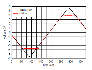
OPA818 D037_OD-Recovery_G=10.gif
G = 10 V/V
Figure 36. Output Overdrive Recovery