SBOS673D September   2017  – December 2018 OPA2837 , OPA837

PRODUCTION DATA.  

  1. Features
  2. Applications
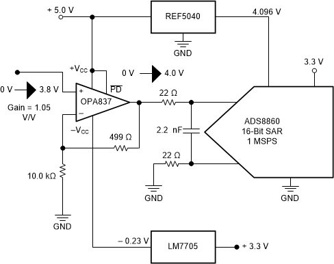
    1.     Low-Power, Low-Noise, Precision, Single-Ended SAR ADC Driver With True Ground Input and Output Range
  3. Description
    1.     Device Images
  4. Revision History
  5. Pin Configuration and Functions
    1.     Pin Functions
  6. Specifications
    1. 6.1  Absolute Maximum Ratings
    2. 6.2  ESD Ratings
    3. 6.3  Recommended Operating Conditions
    4. 6.4  Thermal Information: OPA837
    5. 6.5  Thermal Information: OPA2837
    6. 6.6  Electrical Characteristics: VS = 5 V
    7. 6.7  Electrical Characteristics: VS = 3 V
    8. 6.8  Typical Characteristics: VS = 5.0 V
    9. 6.9  Typical Characteristics: VS = 3.0 V
    10. 6.10 Typical Characteristics: ±2.5-V to ±1.5-V Split Supply
  7. Detailed Description
    1. 7.1 Overview
    2. 7.2 Functional Block Diagrams
    3. 7.3 Feature Description
      1. 7.3.1 OPA837 Comparison
      2. 7.3.2 Input Common-Mode Voltage Range
      3. 7.3.3 Output Voltage Range
      4. 7.3.4 Power-Down Operation
      5. 7.3.5 Low-Power Applications and the Effects of Resistor Values on Bandwidth
      6. 7.3.6 Driving Capacitive Loads
    4. 7.4 Device Functional Modes
      1. 7.4.1 Split-Supply Operation (±1.35 V to ±2.7 V)
      2. 7.4.2 Single-Supply Operation (2.7 V to 5.4 V)
  8. Application and Implementation
    1. 8.1 Application Information
      1. 8.1.1  Noninverting Amplifier
      2. 8.1.2  Inverting Amplifier
      3. 8.1.3  Output DC Error Calculations
      4. 8.1.4  Output Noise Calculations
      5. 8.1.5  Instrumentation Amplifier
      6. 8.1.6  Attenuators
      7. 8.1.7  Differential to Single-Ended Amplifier
      8. 8.1.8  Differential-to-Differential Amplifier
      9. 8.1.9  Pulse Application With Single-Supply Circuit
      10. 8.1.10 ADC Driver Performance
    2. 8.2 Typical Applications
      1. 8.2.1 Active Filters
        1. 8.2.1.1 Design Requirements
        2. 8.2.1.2 Detailed Design Procedure
        3. 8.2.1.3 Application Curves
      2. 8.2.2 Implementing a 2:1 Active Multiplexer
        1. 8.2.2.1 Design Requirements
        2. 8.2.2.2 Detailed Design Procedure
      3. 8.2.3 1-Bit PGA Operation
        1. 8.2.3.1 Design Requirements
        2. 8.2.3.2 Detailed Design Procedure
  9. Power Supply Recommendations
  10. 10Layout
    1. 10.1 Layout Guidelines
    2. 10.2 Layout Example
  11. 11Device and Documentation Support
    1. 11.1 Documentation Support
      1. 11.1.1 Related Documentation
    2. 11.2 Related Links
    3. 11.3 Receiving Notification of Documentation Updates
    4. 11.4 Community Resources
    5. 11.5 Trademarks
    6. 11.6 Electrostatic Discharge Caution
    7. 11.7 Glossary
  12. 12Mechanical, Packaging, and Orderable Information

Package Options

Mechanical Data (Package|Pins)
Thermal pad, mechanical data (Package|Pins)
Orderable Information

Applications

  • 12-Bit to 16-Bit, Low-Power SAR Drivers
  • Precision ADC Reference Buffers
  • Very-Low-Power Active Filters
  • Low-Power Transimpedance Amplifiers
  • Sensor Signal Conditioning
  • Wearable Devices
  • Low-Side Current Sensing

Low-Power, Low-Noise, Precision, Single-Ended SAR ADC Driver With True Ground Input and Output Range

OPA837 OPA2837 OPA837-front-page-diagram-sbos673.gif