SBOSA57B February 2021 – January 2023 OPA855-Q1
PRODUCTION DATA
- 1 Features
- 2 Applications
- 3 Description
- 4 Revision History
- 5 Device Comparison Table
- 6 Pin Configuration and Functions
- 7 Specifications
- 8 Parameter Measurement Information
- 9 Detailed Description
- 10Application, Implementation, and Layout
- 11Power Supply Recommendations
- 12Layout
- 13Device and Documentation Support
- 14Mechanical, Packaging, and Orderable Information
Package Options
Mechanical Data (Package|Pins)
- DSG|8
Thermal pad, mechanical data (Package|Pins)
- DSG|8
Orderable Information
9.3.2 Feedback Pin
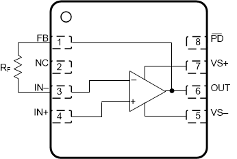
The OPA855-Q1 pin layout is optimized to minimize parasitic inductance and capacitance, which is a critical care about in high-speed analog design. The FB pin (pin 1) is internally connected to the output of the amplifier. The FB pin is separated from the inverting input of the amplifier (pin 3) by a no connect (NC) pin (pin 2). The NC pin must be left floating. There are two advantages to this pin layout:
- A feedback resistor (RF) can connect between the FB and IN– pin on the same side of the package (see Figure 9-4) rather than going around the package.
- The isolation created by the NC pin minimizes the capacitive coupling between the FB and IN– pins by increasing the physical separation between the pins.
 Figure 9-4 RF Connection Between FB and IN– Pins