SBOSA57B February 2021 – January 2023 OPA855-Q1
PRODUCTION DATA
- 1 Features
- 2 Applications
- 3 Description
- 4 Revision History
- 5 Device Comparison Table
- 6 Pin Configuration and Functions
- 7 Specifications
- 8 Parameter Measurement Information
- 9 Detailed Description
- 10Application, Implementation, and Layout
- 11Power Supply Recommendations
- 12Layout
- 13Device and Documentation Support
- 14Mechanical, Packaging, and Orderable Information
Package Options
Mechanical Data (Package|Pins)
- DSG|8
Thermal pad, mechanical data (Package|Pins)
- DSG|8
Orderable Information
9.3.3 Wide Gain-Bandwidth Product
Figure 7-10 shows the open-loop magnitude and phase response of the OPA855-Q1. Calculate the gain bandwidth product of any op amp by determining the frequency at which the AOL is 40 dB and multiplying that frequency by a factor of 100. The open-loop response shows the OPA855-Q1 to have approximately 62° of phase-margin in a noise gain of 7 V/V. The second pole in the AOL response occurs before the magnitude crosses 0 dB, and the resultant phase margin is less than 0°. This indicates instability at a gain of 0 dB (1 V/V). Amplifiers that are not unity-gain stable are known as decompensated amplifiers. Decompensated amplifiers typically have higher gain-bandwidth product, higher slew rate, and lower voltage noise, compared to a unity-gain stable amplifier with the same amount of quiescent power consumption.
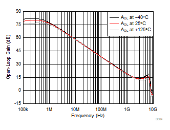
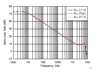
Figure 9-5 shows the open-loop magnitude (AOL) of the OPA855-Q1 as a function of temperature. The results show approximately 5° of phase-margin variation over the entire temperature range in a noise gain of 7 V/V. Semiconductor process variation is the naturally occurring variation in the attributes of a transistor (Early-voltage, β, channel-length and width) and other passive elements (resistors and capacitors) when fabricated into an integrated circuit. The process variation can occur across devices on a single wafer or across devices over multiple wafer lots over time. Typically, the variation across a single wafer is tightly controlled. Figure 9-6 shows the AOL magnitude of the OPA855-Q1 as a function of process variation over time. The results show the AOL curve for the nominal process corner and the variation one standard deviation from the nominal. The simulated results show less than 2° of phase-margin difference within a standard deviation of process variation in a noise gain of 7 V/V.
One of the primary applications for the OPA855-Q1 is as a high-speed transimpedance amplifier (TIA). The low-frequency noise gain of a TIA is 0 dB (1 V/V). At high frequencies the ratio of the total input capacitance and the feedback capacitance set the noise gain. To maximize the TIA closed-loop bandwidth, the feedback capacitance is typically smaller than the input capacitance, which implies that the high-frequency noise gain is greater than 0 dB. As a result, op amps configured as TIAs are not required to be unity-gain stable, which makes a decompensated amplifier a viable option for a TIA. What You Need To Know About Transimpedance Amplifiers – Part 1 and What You Need To Know About Transimpedance Amplifiers – Part 2 describe transimpedance amplifier compensation in greater detail.
 Figure 9-5 Open-Loop Gain vs Temperature
 Figure 9-6 Open-Loop Gain vs Process Variation